Motorola TMS320C6711D warranty Power-down mode logic

Models: TMS320C6711D

1 107
Download 107 pages 8.75 Kb
Page 54
Image 54

SPRS292A − OCTOBER 2005 − REVISED NOVEMBER 2005

power-down mode logic

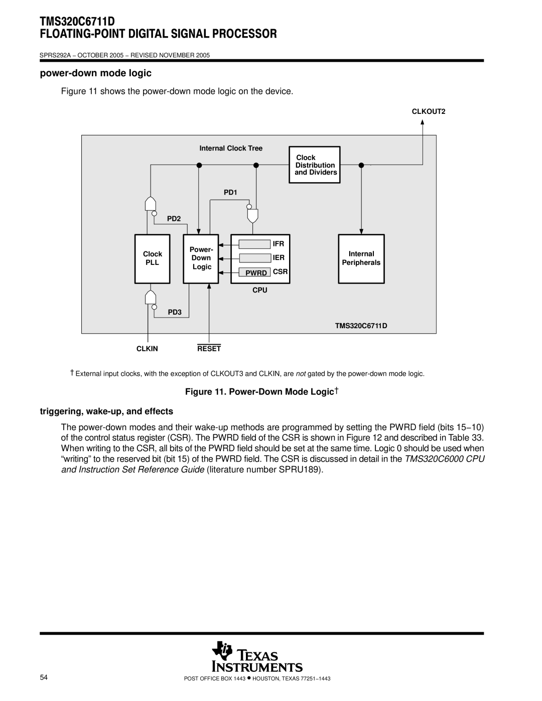
Figure 11 shows the power-down mode logic on the device.

CLKOUT2

Internal Clock Tree

PD1

PD2

Clock

Distribution

and Dividers

Clock

PLL

PD3

IFR

Power-

Down IER

Logic

PWRD CSR

CPU

Internal

Peripherals

TMS320C6711D

CLKINRESET

External input clocks, with the exception of CLKOUT3 and CLKIN, are not gated by the power-down mode logic.

Figure 11. Power-Down Mode Logic

triggering, wake-up, and effects

The power-down modes and their wake-up methods are programmed by setting the PWRD field (bits 15−10) of the control status register (CSR). The PWRD field of the CSR is shown in Figure 12 and described in Table 33. When writing to the CSR, all bits of the PWRD field should be set at the same time. Logic 0 should be used when “writing” to the reserved bit (bit 15) of the PWRD field. The CSR is discussed in detail in the TMS320C6000 CPU and Instruction Set Reference Guide (literature number SPRU189).

54

POST OFFICE BOX 1443 HOUSTON, TEXAS 77251−1443

Page 54
Image 54
Motorola TMS320C6711D warranty Power-down mode logic