SPRS292A − OCTOBER 2005 − REVISED NOVEMBER 2005
RESET TIMING (CONTINUED)
Phase 1 |
| Phase 2 |
|
|
|
| Phase 3 | ||
|
|
CLKIN
ECLKIN
1
RESET
2
Internal Reset
Internal SYSCLK1
Internal SYSCLK2
Internal SYSCLK3
ECLKOUT | 3 | 4 |
|
| |
| 5 | 6 |
CLKOUT2 |
|
|
CLKOUT3 | 7 | 8 |
|
| |
EMIF Z Group† | 9 | 2 |
|
| |
EMIF Low Group† | 10 | 2 |
|
| |
Z Group† | 11 | 2 |
|
| |
| 12 |
|
Z Group 2† |
| 14 |
Boot and Device |
| 13 |
Configuration Pins‡ |
|
|
†EMIF Z group consists of: | EA[21:2], ED[31:0], CE[3:0], BE[3:0], ARE/SDCAS/SSADS, AWE/SDWE/SSWE, AOE/SDRAS/SSOE and | |
| HOLDA |
|
EMIF low group consists of: BUSREQ |
| |
Z group 1 consists of: | CLKR0, CLKR1, CLKX0, CLKX1, FSR0, FSR1, FSX0, FSX1, DX0, DX1, TOUT0, and TOUT1. | |
Z group 2 consists of: | All other HPI and GPIO signals | |
‡Boot and device configurations consist of: HD[8, 4:3].
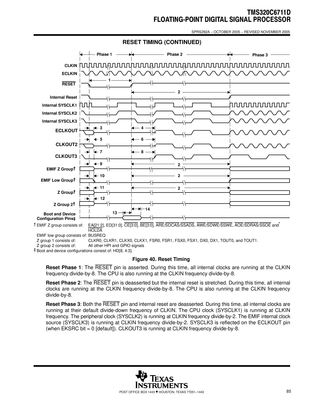
Figure 40. Reset Timing
Reset Phase 1: The RESET pin is asserted. During this time, all internal clocks are running at the CLKIN frequency
Reset Phase 2: The RESET pin is deasserted but the internal reset is stretched. During this time, all internal clocks are running at the CLKIN frequency
Reset Phase 3: Both the RESET pin and internal reset are deasserted. During this time, all internal clocks are running at their default
POST OFFICE BOX 1443 • HOUSTON, TEXAS 77251−1443 | 85 |
