SPRS292A − OCTOBER 2005 − REVISED NOVEMBER 2005
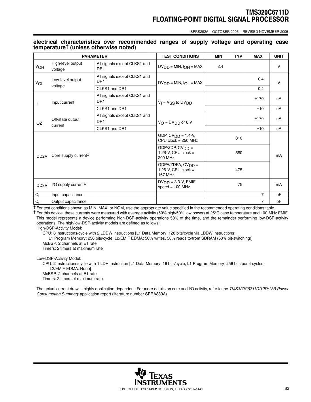
electrical characteristics over recommended ranges of supply voltage and operating case temperature† (unless otherwise noted)
| PARAMETER | TEST CONDITIONS | MIN | TYP | MAX | UNIT | |
|
|
|
|
|
|
|
|
VOH | All signals except CLKS1 and | DVDD = MIN, IOH = MAX | 2.4 |
|
| V | |
voltage | DR1 |
|
| ||||
|
|
|
|
|
| ||
|
|
|
|
|
|
|
|
| All signals except CLKS1 and |
|
|
| 0.4 |
| |
VOL | DR1 | DVDD = MIN, IOL = MAX |
|
| V | ||
voltage |
|
|
| ||||
|
|
|
| ||||
| CLKS1 and DR1 |
|
|
| 0.4 |
| |
|
|
|
|
|
| ||
|
|
|
|
|
|
|
|
|
| All signals except CLKS1 and |
|
|
| ±170 | uA |
II | Input current | DR1 | VI = VSS to DVDD |
|
| ||
|
|
|
| ||||
|
| CLKS1 and DR1 |
|
|
| ±10 | uA |
|
|
|
|
|
|
|
|
| All signals except CLKS1 and |
|
|
| ±170 | uA | |
IOZ | DR1 | VO = DVDD or 0 V |
|
| |||
current |
|
|
|
| |||
| CLKS1 and DR1 |
|
|
| ±10 | uA | |
|
|
|
|
| |||
|
|
|
|
|
|
|
|
|
|
| GDP, CVDD = |
| 810 |
|
|
|
|
| CPU clock = 250 MHz |
|
|
| |
|
|
|
|
|
|
| |
|
|
|
|
|
|
|
|
|
|
| GDP/ZDP, CVDD = |
|
|
|
|
I | Core supply current‡ |
|
| 560 |
| mA | |
|
|
|
|
| |||
DD2V |
|
| 200 MHz |
|
|
|
|
|
|
|
|
|
|
| |
|
|
| GDPA/ZDPA, CVDD = |
|
|
|
|
|
|
|
| 475 |
|
| |
|
|
| 167 MHz |
|
|
|
|
|
|
|
|
|
|
|
|
I | I/O supply current‡ |
| DVDD = |
| 75 |
| mA |
DD3V |
|
| speed = 100 MHz |
|
|
|
|
|
|
|
|
|
|
| |
|
|
|
|
|
|
|
|
Ci | Input capacitance |
|
|
|
| 7 | pF |
Co | Output capacitance |
|
|
|
| 7 | pF |
†For test conditions shown as MIN, MAX, or NOM, use the appropriate value specified in the recommended operating conditions table.
‡For this device, these currents were measured with average activity (50% high/50% low power) at 25°C case temperature and
CPU: 8 instructions/cycle with 2 LDDW instructions [L1 Data Memory: 128 bits/cycle via LDDW instructions;
L1 Program Memory: 256 bits/cycle; L2/EMIF EDMA: 50% writes, 50% reads to/from SDRAM (50%
Timers: 2 timers at maximum rate
CPU: 2 instructions/cycle with 1 LDH instruction [L1 Data Memory: 16 bits/cycle; L1 Program Memory: 256 bits per 4 cycles; L2/EMIF EDMA: None]
McBSP: 2 channels at E1 rate
Timers: 2 timers at maximum rate
The actual current draw is highly
POST OFFICE BOX 1443 • HOUSTON, TEXAS 77251−1443 | 63 |