SPRS292A − OCTOBER 2005 − REVISED NOVEMBER 2005
general-purpose input/output (GPIO)
To use the GP[7:4, 2]
GPxEN = | 1 | GP[x] pin is enabled |
GPxDIR = | 0 | GP[x] pin is an input |
GPxDIR = | 1 | GP[x] pin is an output |
where “x” represents one of the 7 through 4, or 2 GPIO pins
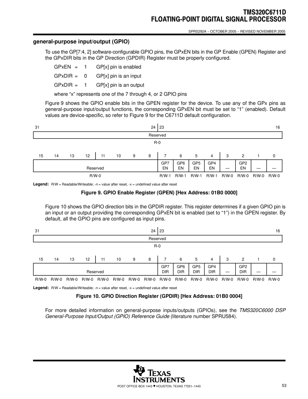
Figure 9 shows the GPIO enable bits in the GPEN register for the device. To use any of the GPx pins as general-purpose input/output functions, the corresponding GPxEN bit must be set to “1” (enabled). Default values are device-specific, so refer to Figure 9 for the C6711D default configuration.
31 |
|
|
|
|
|
|
| 24 | 23 |
|
|
|
|
|
|
| 16 |
|
|
|
|
|
|
|
|
|
|
|
|
|
|
|
|
|
|
|
|
|
|
|
|
|
| Reserved |
|
|
|
|
|
|
|
| |
|
|
|
|
|
|
|
|
|
|
|
|
|
|
|
|
| |
|
|
|
|
|
|
|
|
|
|
|
|
|
|
|
| ||
15 | 14 | 13 | 12 |
| 11 | 10 | 9 | 8 |
| 6 | 5 | 4 |
| 3 | 2 | 1 | 0 |
| 7 |
| |||||||||||||||
|
|
|
|
|
|
|
|
|
|
|
|
|
|
|
|
|
|
|
|
|
|
|
|
|
|
| GP7 | GP6 | GP5 | GP4 |
|
| GP2 |
|
|
|
|
| Reserved |
|
|
| EN | EN | EN | EN |
| — | EN | — | — | ||
|
|
|
|
|
|
|
|
|
|
|
|
|
|
|
|
| |
|
|
|
|
|
|
|
| ||||||||||
Legend: R/W = Readable/Writeable;
Figure 9. GPIO Enable Register (GPEN) [Hex Address: 01B0 0000]
Figure 10 shows the GPIO direction bits in the GPDIR register. This register determines if a given GPIO pin is an input or an output providing the corresponding GPxEN bit is enabled (set to “1”) in the GPEN register. By default, all the GPIO pins are configured as input pins.
31 |
|
|
|
|
|
| 24 | 23 |
|
|
|
|
|
|
| 16 |
|
|
|
|
|
|
|
|
|
|
|
|
|
|
|
|
|
|
|
|
|
|
|
| Reserved |
|
|
|
|
|
|
|
| |
|
|
|
|
|
|
|
|
|
|
|
|
|
|
|
| |
|
|
|
|
|
|
|
|
|
|
|
|
|
|
| ||
15 | 14 | 13 | 12 |
| 10 | 9 | 8 |
| 6 | 5 | 4 |
| 3 | 2 | 1 | 0 |
11 | 7 |
| ||||||||||||||
|
|
|
|
|
|
|
|
|
|
|
|
|
|
|
|
|
|
|
|
|
|
|
|
| GP7 | GP6 | GP5 | GP4 |
|
| GP2 |
|
|
|
|
| Reserved |
|
|
| DIR | DIR | DIR | DIR |
| — | DIR | — | — | |
|
|
|
|
|
|
|
|
|
|
|
|
|
|
|
|
|
| ||||||||||||||||
Legend: R/W = Readable/Writeable;
Figure 10. GPIO Direction Register (GPDIR) [Hex Address: 01B0 0004]
For more detailed information on
POST OFFICE BOX 1443 • HOUSTON, TEXAS 77251−1443 | 53 |