SPRS292A − OCTOBER 2005 − REVISED NOVEMBER 2005
PLL and PLL controller (continued)
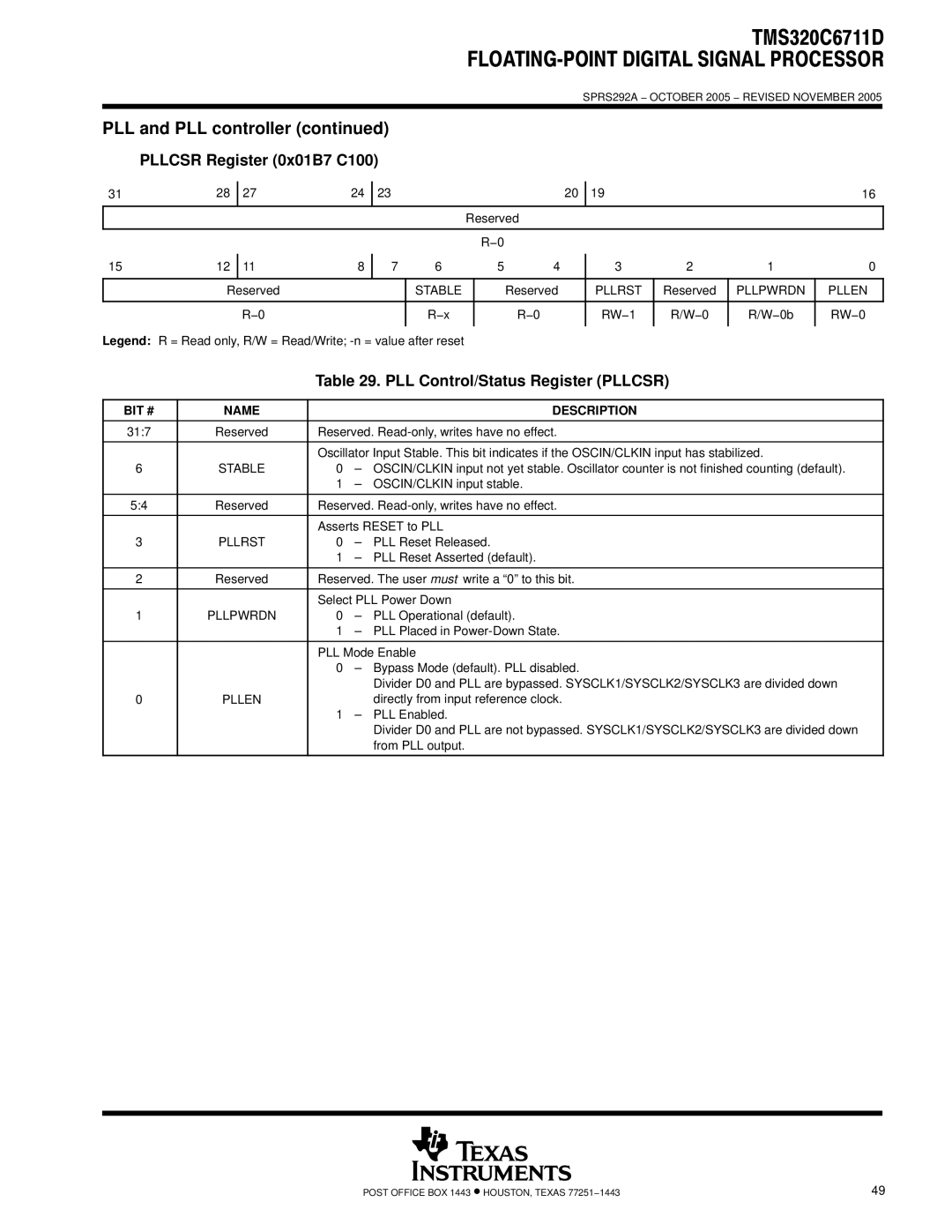
PLLCSR Register (0x01B7 C100)
31 | 28 | 27 | 24 | 23 |
|
|
| 20 | 19 |
|
| 16 |
|
|
|
|
|
|
|
|
|
|
|
| |
|
|
|
|
|
| Reserved |
|
|
|
| ||
|
|
|
|
|
|
|
|
|
|
|
|
|
|
|
|
|
|
|
| R−0 |
|
|
|
|
|
15 | 12 |
| 8 |
| 6 | 5 | 4 |
| 2 | 1 | 0 | |
11 | 7 | 3 | ||||||||||
|
|
|
|
|
|
|
|
|
|
|
|
|
| Reserved |
|
| STABLE |
|
| Reserved | PLLRST | Reserved | PLLPWRDN | PLLEN | |
|
|
|
|
|
|
|
|
|
|
|
|
|
|
| R−0 |
|
| R−x |
|
| R−0 | RW−1 | R/W−0 | R/W−0b | RW−0 |
|
|
|
|
|
|
|
|
|
|
|
|
|
Legend: R = Read only, R/W = Read/Write;
Table 29. PLL Control/Status Register (PLLCSR)
BIT # | NAME |
|
| DESCRIPTION |
|
|
| ||
31:7 | Reserved | Reserved. | ||
|
|
| ||
|
| Oscillator Input Stable. This bit indicates if the OSCIN/CLKIN input has stabilized. | ||
6 | STABLE | 0 | – OSCIN/CLKIN input not yet stable. Oscillator counter is not finished counting (default). | |
|
| 1 | – | OSCIN/CLKIN input stable. |
|
|
| ||
5:4 | Reserved | Reserved. | ||
|
|
| ||
|
| Asserts RESET to PLL | ||
3 | PLLRST | 0 | – | PLL Reset Released. |
|
| 1 | – PLL Reset Asserted (default). | |
|
|
| ||
2 | Reserved | Reserved. The user must write a “0” to this bit. | ||
|
|
| ||
|
| Select PLL Power Down | ||
1 | PLLPWRDN | 0 | – | PLL Operational (default). |
|
| 1 | – PLL Placed in | |
|
|
| ||
|
| PLL Mode Enable | ||
|
| 0 | – Bypass Mode (default). PLL disabled. | |
|
|
|
| Divider D0 and PLL are bypassed. SYSCLK1/SYSCLK2/SYSCLK3 are divided down |
0 | PLLEN |
|
| directly from input reference clock. |
|
| 1 | – | PLL Enabled. |
|
|
|
| Divider D0 and PLL are not bypassed. SYSCLK1/SYSCLK2/SYSCLK3 are divided down |
|
|
|
| from PLL output. |
|
|
|
|
|
POST OFFICE BOX 1443 • HOUSTON, TEXAS 77251−1443 | 49 |
