SPRS292A − OCTOBER 2005 − REVISED NOVEMBER 2005
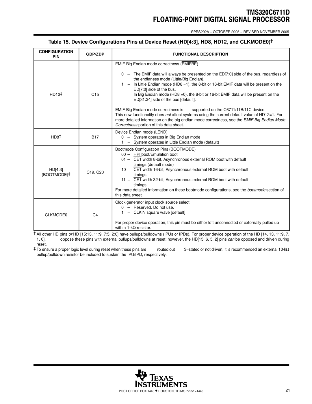
Table 15. Device Configurations Pins at Device Reset (HD[4:3], HD8, HD12, and CLKMODE0)†
CONFIGURATION | GDP/ZDP |
|
| FUNCTIONAL DESCRIPTION | ||
PIN |
|
| ||||
|
|
|
|
|
| |
|
|
| ||||
|
| EMIF Big Endian mode correctness |
|
| ||
|
| (EMIFBE) |
| |||
|
| 0 | – | The EMIF data will always be presented on the ED[7:0] side of the bus, regardless of | ||
|
|
|
| the endianess mode (Little/Big Endian). | ||
|
| 1 | − | In Little Endian mode (HD8 =1), the | ||
HD12‡ |
|
|
| ED[7:0] side of the bus. | ||
C15 |
|
| In Big Endian mode (HD8 =0), the | |||
|
|
|
| ED[31:24] side of the bus [default]. | ||
|
| EMIF Big Endian mode correctness is not supported on the C6711/11B/11C device. | ||||
|
| This new functionality does not affect systems using the current default value of HD12=1. For | ||||
|
| more detailed information on the big endian mode correctness, see the EMIF Big Endian Mode | ||||
|
| Correctness portion of this data sheet. | ||||
|
|
| ||||
HD8‡ |
| Device Endian mode (LEND) | ||||
B17 | 0 | – | System operates in Big Endian mode | |||
|
| 1 | − | System operates in Little Endian mode (default) | ||
|
|
| ||||
|
| Bootmode Configuration Pins (BOOTMODE) | ||||
|
| 00 – | HPI boot/Emulation boot | |||
|
| 01 – | CE1 width | |||
|
|
|
| timings (default mode) | ||
HD[4:3] | C19, C20 | 10 − | CE1 width | |||
(BOOTMODE)‡ |
|
| timings | |||
|
|
| ||||
|
| 11 − | CE1 width | |||
|
|
|
| timings | ||
|
| For more detailed information on these bootmode configurations, see the bootmode section of | ||||
|
| this data sheet. | ||||
|
|
| ||||
|
| Clock generator input clock source select | ||||
|
| 0 | – | Reserved. Do not use. | ||
CLKMODE0 | C4 | 1 | − | CLKIN square wave [default] | ||
|
|
|
|
| ||
|
| For proper device operation, this pin must be either left unconnected or externally pulled up | ||||
|
| with a | ||||
†All other HD pins or HD [15:13, 11:9, 7:5, 2:0] have pullups/pulldowns (IPUs or IPDs). For proper device operation of the HD [14, 13, 11:9, 7, 1, 0], do not oppose these pins with external pullups/pulldowns at reset; however, the HD[15, 6, 5, 2] pins can be opposed and driven during reset.
‡To ensure a proper logic level during reset when these pins are both routed out and 3−stated or not driven, it is recommended an external
POST OFFICE BOX 1443 • HOUSTON, TEXAS 77251−1443 | 21 |