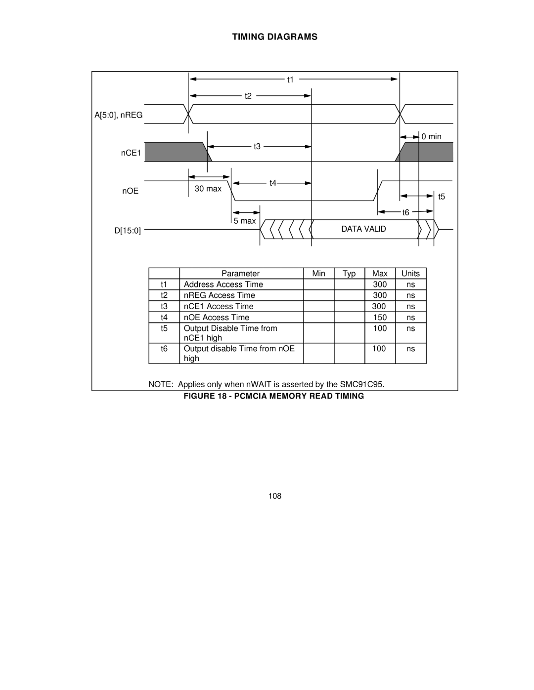
TIMING DIAGRAMS
A[5:0], nREG
nCE1
nOE
D[15:0]
t1
t2
t3
t4
30 max
5 max

 0 min
0 min
t5
![]() t6
t6 ![]()
DATA VALID
| Parameter | Min | Typ | Max | Units |
t1 | Address Access Time |
|
| 300 | ns |
t2 | nREG Access Time |
|
| 300 | ns |
t3 | nCE1 Access Time |
|
| 300 | ns |
t4 | nOE Access Time |
|
| 150 | ns |
t5 | Output Disable Time from |
|
| 100 | ns |
| nCE1 high |
|
|
|
|
t6 | Output disable Time from nOE |
|
| 100 | ns |
| high |
|
|
|
|
NOTE: Applies only when nWAIT is asserted by the SMC91C95.