www.ti.com | Architecture |
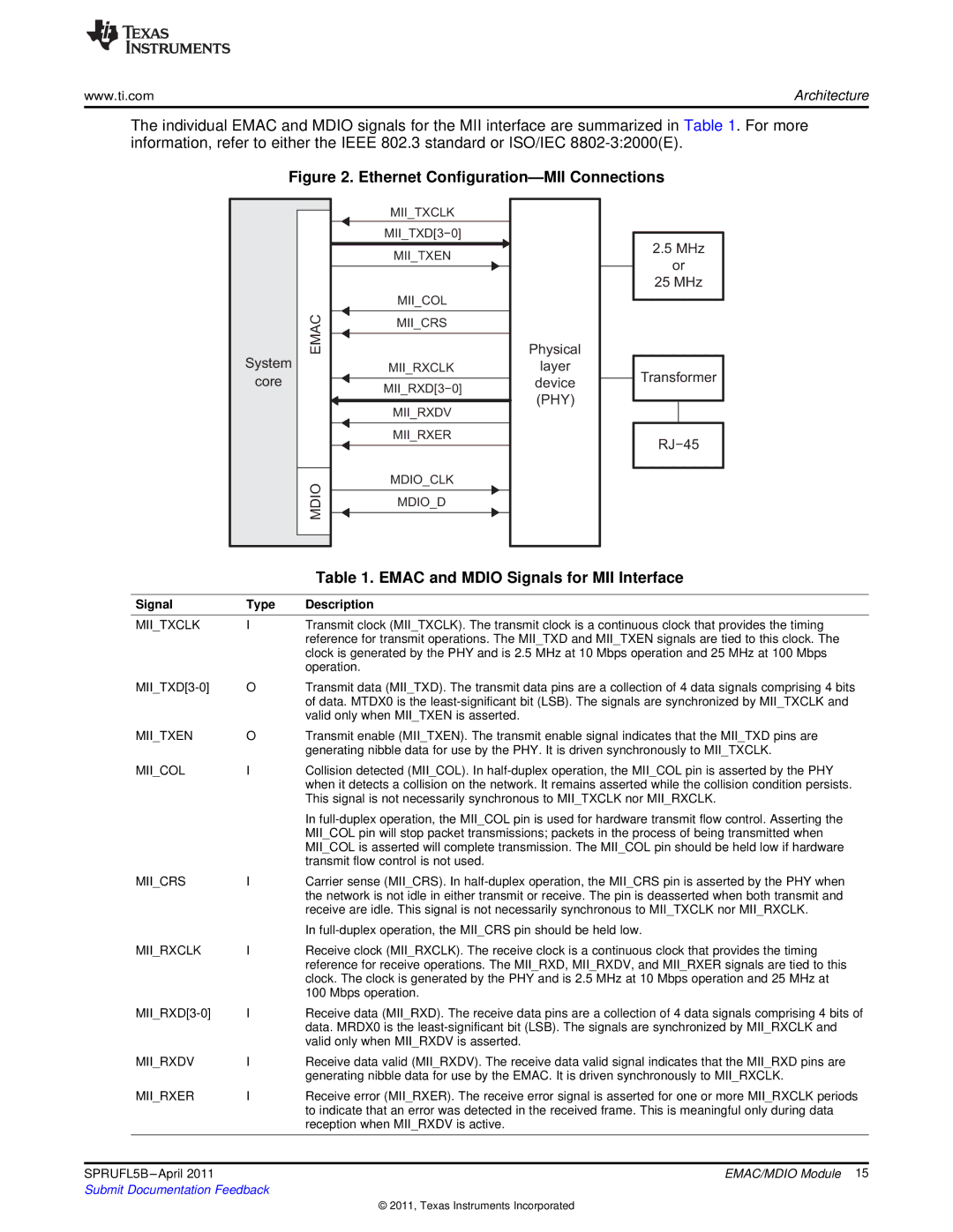
The individual EMAC and MDIO signals for the MII interface are summarized in Table 1. For more information, refer to either the IEEE 802.3 standard or ISO/IEC
Figure 2. Ethernet Configuration—MII Connections
System
core
EMAC
MDIO
MII_TXCLK
MII_TXD[3−0]
MII_TXEN
MII_COL
MII_CRS
MII_RXCLK
MII_RXD[3−0]
MII_RXDV
MII_RXER
MDIO_CLK
MDIO_D
Physical layer device (PHY)
2.5MHz or
25 MHz
Transformer
RJ−45
|
|
| Table 1. EMAC and MDIO Signals for MII Interface |
|
|
|
|
| Signal | Type | Description |
|
|
|
|
| MII_TXCLK | I | Transmit clock (MII_TXCLK). The transmit clock is a continuous clock that provides the timing |
|
|
| reference for transmit operations. The MII_TXD and MII_TXEN signals are tied to this clock. The |
|
|
| clock is generated by the PHY and is 2.5 MHz at 10 Mbps operation and 25 MHz at 100 Mbps |
|
|
| operation. |
| O | Transmit data (MII_TXD). The transmit data pins are a collection of 4 data signals comprising 4 bits | |
|
|
| of data. MTDX0 is the |
|
|
| valid only when MII_TXEN is asserted. |
| MII_TXEN | O | Transmit enable (MII_TXEN). The transmit enable signal indicates that the MII_TXD pins are |
|
|
| generating nibble data for use by the PHY. It is driven synchronously to MII_TXCLK. |
| MII_COL | I | Collision detected (MII_COL). In |
|
|
| when it detects a collision on the network. It remains asserted while the collision condition persists. |
|
|
| This signal is not necessarily synchronous to MII_TXCLK nor MII_RXCLK. |
|
|
| In |
|
|
| MII_COL pin will stop packet transmissions; packets in the process of being transmitted when |
|
|
| MII_COL is asserted will complete transmission. The MII_COL pin should be held low if hardware |
|
|
| transmit flow control is not used. |
| MII_CRS | I | Carrier sense (MII_CRS). In |
|
|
| the network is not idle in either transmit or receive. The pin is deasserted when both transmit and |
|
|
| receive are idle. This signal is not necessarily synchronous to MII_TXCLK nor MII_RXCLK. |
|
|
| In |
| MII_RXCLK | I | Receive clock (MII_RXCLK). The receive clock is a continuous clock that provides the timing |
|
|
| reference for receive operations. The MII_RXD, MII_RXDV, and MII_RXER signals are tied to this |
|
|
| clock. The clock is generated by the PHY and is 2.5 MHz at 10 Mbps operation and 25 MHz at |
|
|
| 100 Mbps operation. |
| I | Receive data (MII_RXD). The receive data pins are a collection of 4 data signals comprising 4 bits of | |
|
|
| data. MRDX0 is the |
|
|
| valid only when MII_RXDV is asserted. |
| MII_RXDV | I | Receive data valid (MII_RXDV). The receive data valid signal indicates that the MII_RXD pins are |
|
|
| generating nibble data for use by the EMAC. It is driven synchronously to MII_RXCLK. |
| MII_RXER | I | Receive error (MII_RXER). The receive error signal is asserted for one or more MII_RXCLK periods |
|
|
| to indicate that an error was detected in the received frame. This is meaningful only during data |
|
|
| reception when MII_RXDV is active. |
|
|
|
|
|
|
|
|
SPRUFL5B |
| EMAC/MDIO Module 15 | |
Submit Documentation Feedback |
| ||
© 2011, Texas Instruments Incorporated