www.ti.com
PLL Controller Registers
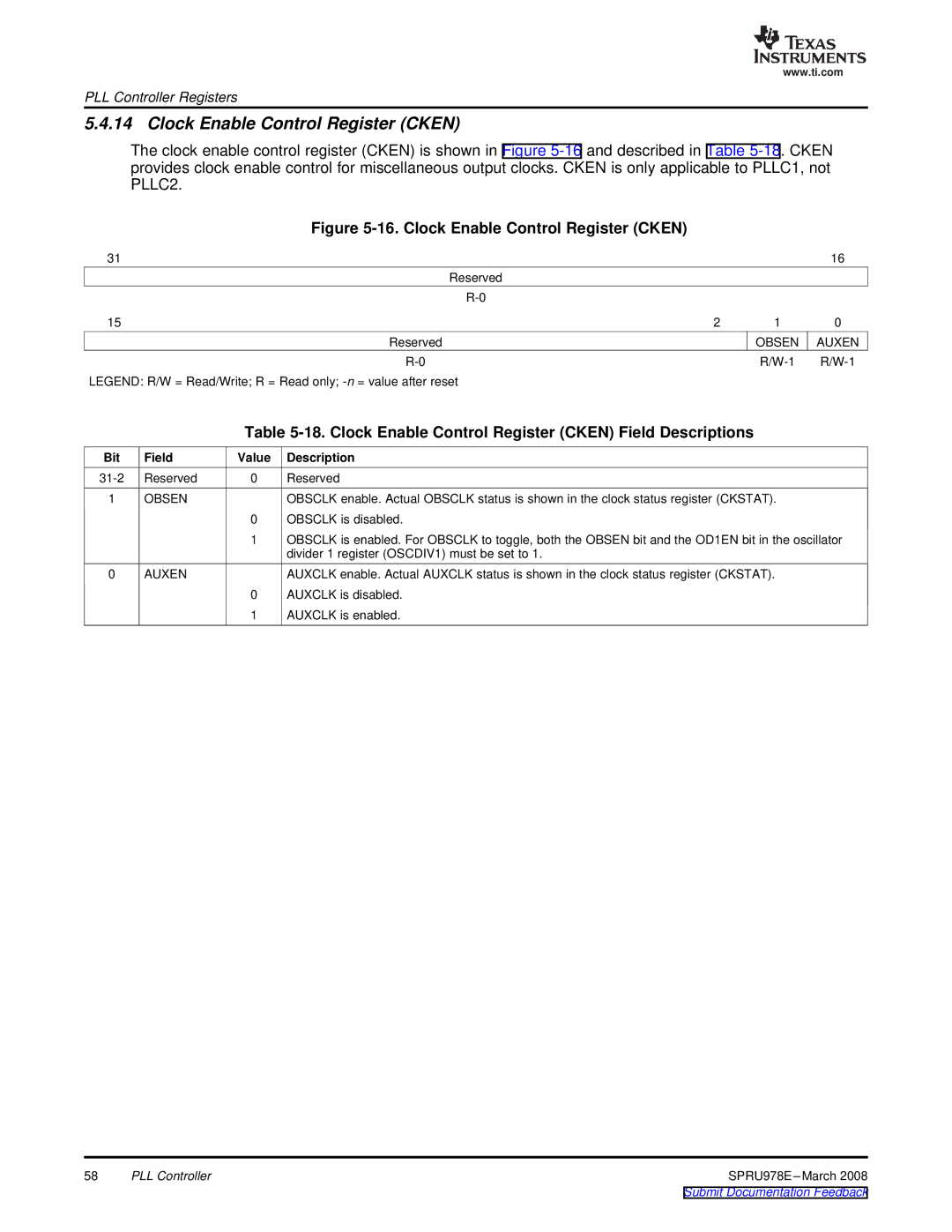
5.4.14 Clock Enable Control Register (CKEN)
The clock enable control register (CKEN) is shown in Figure
Figure 5-16. Clock Enable Control Register (CKEN)
31 |
|
| 16 |
| Reserved |
|
|
|
|
| |
15 | 2 | 1 | 0 |
Reserved |
| OBSEN | AUXEN |
|
LEGEND: R/W = Read/Write; R = Read only;
Table 5-18. Clock Enable Control Register (CKEN) Field Descriptions
Bit | Field | Value | Description |
Reserved | 0 | Reserved | |
1 | OBSEN |
| OBSCLK enable. Actual OBSCLK status is shown in the clock status register (CKSTAT). |
|
| 0 | OBSCLK is disabled. |
1OBSCLK is enabled. For OBSCLK to toggle, both the OBSEN bit and the OD1EN bit in the oscillator divider 1 register (OSCDIV1) must be set to 1.
0 | AUXEN | AUXCLK enable. Actual AUXCLK status is shown in the clock status register (CKSTAT). |
| 0 | AUXCLK is disabled. |
| 1 | AUXCLK is enabled. |
58 | PLL Controller |