www.ti.com
Clock Domains
4.2.5 Video Processing Back End
The video processing back end (VPBE) is a submodule of the video processing subsystem (VPSS). The VPBE must interface with a variety of LCDs, as well as the
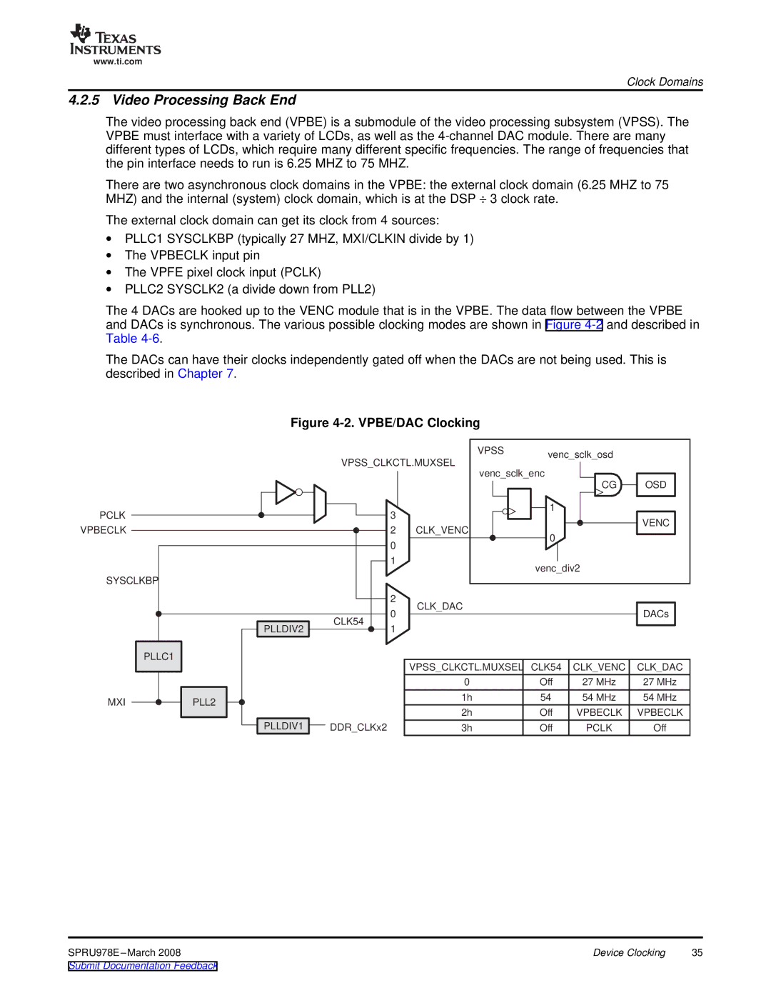
There are two asynchronous clock domains in the VPBE: the external clock domain (6.25 MHZ to 75 MHZ) and the internal (system) clock domain, which is at the DSP ÷ 3 clock rate.
The external clock domain can get its clock from 4 sources:
∙PLLC1 SYSCLKBP (typically 27 MHZ, MXI/CLKIN divide by 1)
∙The VPBECLK input pin
∙The VPFE pixel clock input (PCLK)
∙PLLC2 SYSCLK2 (a divide down from PLL2)
The 4 DACs are hooked up to the VENC module that is in the VPBE. The data flow between the VPBE and DACs is synchronous. The various possible clocking modes are shown in Figure
The DACs can have their clocks independently gated off when the DACs are not being used. This is described in Chapter 7.
Figure |
|
| ||
|
| VPSS | venc_sclk_osd |
|
| VPSS_CLKCTL.MUXSEL |
| ||
|
|
| ||
|
| venc_sclk_enc |
| |
|
|
| CG | OSD |
PCLK | 3 |
| 1 |
|
|
| VENC | ||
VPBECLK | 2 | CLK_VENC |
| |
0 |
| |||
| 0 |
|
| |
|
|
|
| |
| 1 |
| venc_div2 |
|
|
|
|
| |
SYSCLKBP |
|
|
|
|
| 2 | CLK_DAC |
|
|
| 0 |
| DACs | |
|
|
| ||
PLLDIV2 | CLK54 |
|
|
|
1 |
|
|
| |
| PLLC1 |
| VPSS_CLKCTL.MUXSEL | CLK54 CLK_VENC CLK_DAC | ||
|
|
| ||||
|
|
| 0 | Off | 27 MHz | 27 MHz |
MXI | PLL2 |
| 1h | 54 | 54 MHz | 54 MHz |
| 2h | Off | VPBECLK | VPBECLK | ||
|
|
| ||||
| PLLDIV1 | DDR_CLKx2 | 3h | Off | PCLK | Off |
Device Clocking | 35 |
