www.ti.com
PLL2 Control
5.3PLL2 Control
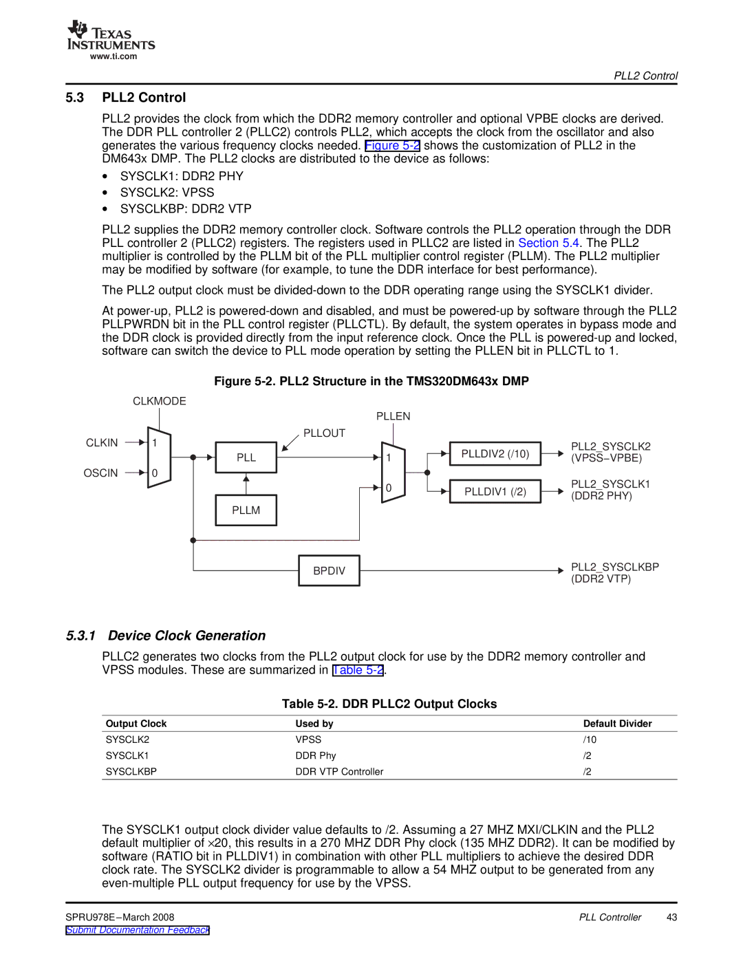
PLL2 provides the clock from which the DDR2 memory controller and optional VPBE clocks are derived. The DDR PLL controller 2 (PLLC2) controls PLL2, which accepts the clock from the oscillator and also generates the various frequency clocks needed. Figure
∙SYSCLK1: DDR2 PHY
∙SYSCLK2: VPSS
∙SYSCLKBP: DDR2 VTP
PLL2 supplies the DDR2 memory controller clock. Software controls the PLL2 operation through the DDR PLL controller 2 (PLLC2) registers. The registers used in PLLC2 are listed in Section 5.4. The PLL2 multiplier is controlled by the PLLM bit of the PLL multiplier control register (PLLM). The PLL2 multiplier may be modified by software (for example, to tune the DDR interface for best performance).
The PLL2 output clock must be
At
Figure 5-2. PLL2 Structure in the TMS320DM643x DMP
| CLKMODE |
|
|
| PLLEN |
CLKIN | 1 | PLLOUT |
| ||
| PLL | 1 |
OSCIN | 0 |
|
|
| 0 |
| PLLM |
|
|
| BPDIV |
PLLDIV2 (/10)
PLLDIV1 (/2)
PLL2_SYSCLK2 (VPSS−VPBE)
PLL2_SYSCLK1 (DDR2 PHY)
PLL2_SYSCLKBP (DDR2 VTP)
5.3.1 Device Clock Generation
PLLC2 generates two clocks from the PLL2 output clock for use by the DDR2 memory controller and VPSS modules. These are summarized in Table
Table 5-2. DDR PLLC2 Output Clocks
Output Clock | Used by | Default Divider |
SYSCLK2 | VPSS | /10 |
SYSCLK1 | DDR Phy | /2 |
SYSCLKBP | DDR VTP Controller | /2 |
The SYSCLK1 output clock divider value defaults to /2. Assuming a 27 MHZ MXI/CLKIN and the PLL2 default multiplier of ×20, this results in a 270 MHZ DDR Phy clock (135 MHZ DDR2). It can be modified by software (RATIO bit in PLLDIV1) in combination with other PLL multipliers to achieve the desired DDR clock rate. The SYSCLK2 divider is programmable to allow a 54 MHZ output to be generated from any
PLL Controller | 43 |