Page
Programmable Peripheral Interface
Clock Generator for 8080A
System Controller for 8080A
Programmable Communication Interface
Contents
Peri pherals
127
Chapter Packaging Information
Page
Microcomputer Design Aids
Advantages of Designing With Microcomputers
Conventional System Programmed Logic
Iii
Applications Example
1IIII~Iff1
Peripheral Devices Encountered
Application
Architecture of a CPU
Typical Computer System
Accumulator
Instruction Register and Decoder
Program Counter Jumps, Subroutines and the Stack
Computer Operations
Control Circuitry
Address Registers
Arithmetic/Logic Unit ALU
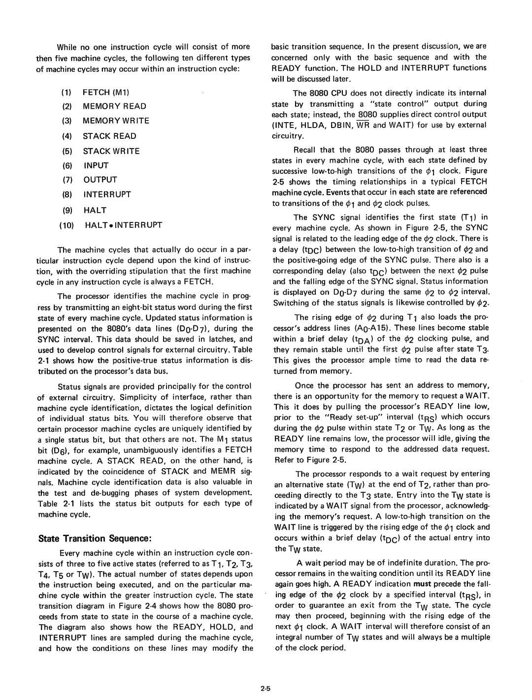
Wait memory synchronization
Instruction Fetch
Memory Read
Memory Write
Page
Page
8080 Photomicrograph With Pin Designations
INTE~
Registers
Architecture of the 8080 CPU
Processor Cycle
Arithmetic and Logic Unit ALU
Instruction Register and Control
Data Bus Buffer
Machine Cycle Identification
Halt
State Transition Sequence
Status Bit Definitions
Status Word Chart
Status Information Definition
?~~
CPU State Transition Diagram
Rr\
ONE ,----- ~
~2. State Definitions
State Associated Activities
Interrupt Sequences
RLrL- rL rL rL-rL- rLrL
¢2 -+--sLJJlL-..rrL~LJLLJTLJJ\.lJL
Halt Sequences
Hold Sequences
START-UP of the 8080 CPU
11. Halt Timing
~~~~t==p
001
STATUS6
Xram
~iA~~~11
~iA~~~11
~iA~~ll,12
~A~~~ll
111 000 001 010 011 100 101
Value
Basic System Operation
Typical Computer System Block Diagram
Clock Generator Design
CPU Module Design
8080 CPU
Clock Generator and High Level Driver
~50ns
ClK 0.......-..-.-----.. tf1A TTL
High Level Driver Design
Ststb !1
Page
ROM Interface
Interfacing the 8080 CPU to Memory and I/O Devices
RAM Interface
Ill
Memory Mapped I/O
Interface
General Theory
Isolated I/O
Interface Example
Addressing
Memr to
15 Format
13 Format
8080 Instruction SET
Instruction and Data Formats
Addressing Modes
Byte One
Byte Two
Byte Three I D7
All
Symbols and Abbreviations
Symbols Meaning
Description Format
Reg. indirect
Content of register r2 is moved to register r1
Data Transfer Group
MOV r1, r2 Move Register
0 I R
0 I R p
0 I 0 o
0 I
Arithmetic Group
1 I
0 I D I D
R 0 I
Cycles States Addressing reg. indirect Flags Z,S,P ,CY,AC
I I
Logical Group
OCR M Decrement memory
1 1 1
I 0 I 1 I 1 I
I 1 I 1 o I 1 I 1 I
~11~
Cycles States Flags none
0 I 1 I
0 I 0 1 I
0 I 0 I
000
Branch Group
Ccondition addr
I c c I c I 0 I 0 I
SP ~ SP +
1 I R
Stack, I/O, and Machine Control Group
I 1 o
Push rp
Cycles States Flags None
Exchange stack top with Hand L
~ SP +
~ data
Instruction SET
Programmable Peripheral Interface
8224 8080A-1 8228 8080A-2 8080A M8080-A
Page
PIN Names
Schottky Bipolar
Clock Generator
Functional Description
General
Oscillator
Ststb Status Strobe
Power-On Reset and Ready Flip-Flops
Crystal Requirements
Characteristics
8pF
Input
TORS tORH tOR FMAX
Characteristics For tCY = 488.28 ns
Example
T42 T01 T02 T03 Toss
Dbin
PIN Configuration Block Diagram
Block
General
Inta None Control
Signals
Hlda to Read Status Outputs
Characteristics TA = Oc to 70C Vee = 5V ±5%
TE~r
Waveforms
VCC=5V
GoUT
Ststb
VTH
GND ---. r
·-c
?oo .H
Intel Silicon Gate MOS 8080 a
Vss
Vee
8080A Functional PIN Definition
IOl = 1.9mA on all outputs
Characteristics
Absolute Maximum RATINGS·
Capacitance
~~1 t CY
=..... -r-DATAIN
~I~~~
Timing Waveforms
Typical ~ Output Delay VS. a Capacitance
Characteristics
Typical Instructions
Instruction SET
Summary of Processor Instructions
Silicon Gate MOS 8080.A
Infel Silicon Gate MOS 8080A-1
Max
Symbol Parameter Typ
Unit
~tOF.I
Fft~l
~-t
TYPICAL!J. Output Delay VS. ~ Capacitance
Infel Silicon Gate MOS 8080 A-2
VAOOR/OATA = VSS + O.45V
+10
Cout
J1A
Unit Test Condition
Symbol Parameter Min
Min. Max. Unit Test Condition
Typical ~ Output Delay VS. ~ Capacitance
Page
Intel . Silicon Gate MOS M8080A
Interrupt instructions
Immediate mode or I/O instructions
Register to regist~r, memory refer
Ence, arithmetic or logical, rotate
Llf17
Summary of Processor Instructions
M8080A Functional PIN Definition
Silicon Gate MOS M8080A
IOL = 1.9mA on all outputs
Absolute Maximum Ratings
Operation
Symbol Parameter Min. Max Unit Test Condition
~I~
Silicon Gate MOS M8080A
Page
ROMs 8702A 8704 8708 8316A
Page
Silicon Gate MOS 8702A
PIN Connections
Operating Characteristics
Voo
= V ce
Switching Characteristics
1N= Vee
~10%
Cs=o.~
\ \
SYMBOLTESTMIN. TYP. MAX. Unit Conditions
Operating Characteristics for Programming Operation
Symbol Test
Characteristics for Programming Operation
Program Operation
Switching Characteristics for Programming Operation
CS = OV
Programming Operation of the 8702A
Programming Instructions for the 8702A
Operation of the 8702A in Program Mode
II. Programming of the 8702A Using Intel Microcomputers
III a Erasing Procedure
Page
PIN Names
PIN Configurations Block Diagram
VOH1
Comment
III
IBB
Max Unit
Symbol Parameter Typ. Max. Unit Conditions
Test Conditions
Waveforms
TpF Program Pulse Fall Time
Parameter Min
Programming Current RnA Program Pulse Amplitude
CS/WE = +12V
Read/Program/Read Transitions
+-------1
PEEEf!1EJEZPlEzz$m=2!·m·· Icc
150 r
Silicon Gate MOS
Outa
Comment
MAX Unit
CS=O.O
100 ns 7001 JJ.s
~~~H --4!~--~N-~-TA-AL-~-DU-T--~\
200ns 500ns 300 ns
Cs .. o.~ ~r
Typical Characteristics
Silicon Gate MOS
ILO
Ilcl
Ilpc
Ilkc
CoUT
Conditions of Test for Characteristics
CIN
~ ~ ~
Customer Number Oate
Mask Option Specifications
Marking
Pppp
79-80
~ r ------ + -- t --- . L . ------ rJ
Title Card
Blank
Intel Silicon Gate MOS ROM 8316A
PIN Configuration Block Diagram
Conditions of Test for
400
CAPACITANCE2 TA = 25C, f = 1 MHz
Waveforms
OU~TVALID
ILICO.N Gate MOS ROM 8316A
Typical D.C. Characteristics
Mask Option Speci Fications
Customer
Number Oate
STO
COM~ANY Name
Title Card
RAMs
Page
Silicon Gate MOS
PIN Configuration Logic Symbol Block Diagram
+----+
~E~~=~utP~-t-·7~igh-~\/oltage-~------ ---- --i2-+---=~== ~=
= OC
10H = -150 p.A
00 ~
Conditions of Test
Page
Silicon Gate MOS
PIN Configuration Logic Symbol Block Diagram
ICC2
Symbol Parameter Min. Typ.r
III
ICC1
Timing Measurement Reference Level Volt
Write 1~-tAW--.I-----I
550 200
Input Pulse Rise and Fall Times 20nsec
Page
Silicon Gate MOS
TA = OOC to +70C, Vee = 5V ±5% unless otherwise specified
Power Dissipation Watt
5V to +7V
Comment
Conditions of Test
85o-·-···T
+--~~~TL~~~EEt~~~P-.±
Capacitance T a = 25C, f = 1MHz
~~~b~.J
Typical A.C. Characteristics
Silicon Gate MOS 8102A-4
TA = OC to +70 o e, Vcc = 5V ±5% unless otherwise specified
230
450
300
Output Source Current VS
VIN Limits VS. Temperature
Access Time VS Ambient Temperature
Access Time VS LOAD·CAPACITANCE
PIN Configuration Logic Symbol Block Diagram
Fully Decoded Random Access BIT Dynamic Memory
IOOAV2
Silicon Gate MOS 81078·4
IMP~ri~~CE
II.~
Write Cycle
Read Cycle
4000
Ref =
Typical Characteristics
RWc 590 CD
Symbol Parameter Min Max
Numbers in parentheses are for minimum cycle timing in ns
System Interfaces and Filtering
Power Dissipation
Standby Power
Refresh
Typical System
BIT 256 x 4 Static Cmos RAM
Icccr
ICC2
VIH VOL VOH
VOR
Timing Measurement Reference Level Volt
Input Pulse Rise and Fall Times 20nsec
~I----- t CW2 ------ . t
Schottky Bipolar
PIN Configuration Logic Symbol
Voo- --- ---T
Conditions of Test
All driver outputs are in the state indicated
Power Supply Current Drain and Power Dissipation
Typical System
Dynamic Memory Refresh Controller
Page
8212 8255 8251
Page
EIGHT-BIT INPUT/OUTPUT Port
PIN Configuration Logic Diagram
OS2
Functional Description
Gated Buffer
Basic Schematic Symbols
II. Gated Buffer 3·STATE
Are 3-state
BI-DIRECTIONAL BUS Driver
III. Bi-Directional Bus Driver
IV. Interrupting Input Port
Interrupt Instruction Port
OvJ \.. -4~
VI. Output Port With Hand-Shaking
VII Status Latch
8080 4
System
Viii System
OUT
Vee
IX System
1G~D L-~
DalN-t?!NrJ
Absolute Maximum Ratings·
Characteristics
052 ~
Typical Characteristics
Tpw
OUT
TA = OC to + 75C Vee = +5V ± 5%
Switching Characteristics
12 pF
~~~lEI~S 1-- +SV
Programmable Peripheral Interface
Basic Functional Description
General
Data Bus Buffer
Read/Write and Control Logic
Ports A, B, and C
Reset
PIN Configuration
Group a and Group B Controls
PA 7 ·pAo
Mode Selection
Single Bit Set/Reset Feature
Detailed Operational Description
Mode 0 Timing
Operating Modes Mode 0 Basic Input/Output
Interrupt Control Functions
Mode 0 Configurations
Mode 0 Port Definition Chart
119
· / ,4
Operating Modes Mode 1 Strobed Input/Output
Inte a
Input Control Signal Definition
IBF Input Buffer Full F/F
Intr Interrupt Request
Intea
Output Control Signal Definition
Output Operations
Combinations of Mode
Bi-Directional Bus I/O Control Signal Definition
Operating Modes
Mode 2 Bi-directional Timing
Mode 2 Control Word
Mode 2 and Mode 0 Output
Mode 2 Combinations
Reading Port C Status
Special Mode Combination Considerations
Mode Definition Summary Table
Source Current Capability on Port B and Port C
Keyboard and Terminal Address Interface
Applications
Printer Interface
Keyboard and Display Interface
~.LEFT/RIGHT
PCO
Silicon Gate MOS
Time From STB = 0 To IBF
Characteristics TA = oc to 70C Vee = +5V ±5% vss = OV
Vil Input Low Voltage
Input High Voltage Val Output Low Voltage IOl = 1.6mA
Mode 0 Basic Input
Mode 1 Strobed Input
Mode 2 Bi-directional
Page
Programmable Communication Interface
ClK Clock
Reset Reset
General
ReadlWrite Control logic
DTR Data Termin·al Ready
Modem Control
DSR Data Set Ready
TxE Transmitter Empty
RxC Receiver Clock
Receiver Buffer
Receiver Control
RxRDY Receiver Ready
Programming
Mode Instruction
Command Instruction
Detailed Operation Description
Data C~~RACTER
Mode Instruction Definition
Asynchronous Mode Transmission
Asynchronous Mode Receive
Synchronous Mode, Transmission Format
Synchronous Mode Transmission
Synchronous Mode Receive
Mode Instruction Format, Synchronous Mode
Status Read Format
Command Instruction Definition
Command Instruction Format
Status Read Definition
Synchronous Interface to Telephone Lines
Asynchronous Serial Interface to CRT Terminal, DC-9600 Baud
Asynchronous Interface to Telephone Lines
Synchronous Interface to Terminal or Peripheral Device
Icc
Capacitance
IOL
Typ
TA = oc to 70C VCC = 5.0V ±5% Vss = OV Symbol Parameter
RXD~
RxD
SRX ~4IlI
~AST BIT ,----1
Peripherals
Page
High Speed 1 OUT of 8 Binary Decoder
Decoder
Enable Gate
System
24K Memory Interface
Using a very similar circuit to the I/O port decoder, an ar
Port Decoder
Chip Select Decoder
Ill
Logic Element Example
\lJ
JJ,.--+-I----.....1
8205
Characteristics TA = OOC to +75C, Vee = 5.0V ±5%
Typical Characteristics
Symbol VOL VOH
Test Waveforms
Switching Characteristics Conditions of Test Test Load
Address or Enable to Output Delay VS. Load Capacitance
Address or Enable to Output Delay VS. Ambient Temperature
~ R
PIN Configuration
~ ~
Polled Method
Interrupts in Microcomputer Systems
Interrupt Method
Current Status Register
Priority Encoder
AO, A1, A2
Control Signals
INTE, elK
ElR, ETlG, ENGl
Basic Operation
Level Controller
Level Controller
I I
Cascading
Absolute Maximum Ratings
Operating Characteristics
Symbol Parameter Limits Unit Conditions Min Typ.£1
Los
Characteristics and Waveforms TA = oc to +70C, vcc = +5V ±5%
Schottky Bipolar
8216 8226
+-......---- n cs
Control Gating OlEN, CS
Bi-Directional Driver
Memory and 1/0 Interface to a Bi-directional Bus
Applications of 8216/8226
Large microcomputer systems it is often necessary to pro
Input Leakage Current OlEN, CS VR =5.25V
IcC Power Supply Current 120
Input Load Current OlEN, CS VF =0.45
Input Load Current All Other Inputs VF =0.45
OUT
Waveforms
Page
8253 8257 8259
Page
It uses nMOS technology ~Jmodesof operation are
Programmable Interval Timer
System Interface
Block Diagram
Preliminary Functional Description
System Interface
Programmable DMA Controller
Dack 2
System Interface
System Application
CS-------It
LJJ
Intel
CPU Group
ROMs RAMs
Peripheral Coming Soon
735~
~~~1
It-j
Lead CerDIP Dual IN-LINE Package D
\.--.J.. ~~~l
·34o~
Lead Plastic Dual IN-LINE Package P
Sales and Marketing Offices
Distributors
Page
Page
Page
Page
Page
Page
Instruction SET
Summary of Processor Instructions By Alphabetical Order
Instruction SET
Microcomputer System Users Registration Card
Microcomputer Systems Bowers Avenue Santa Clara, CA
Intel Corporation
Inter