TMS320C67x/C67x+ DSP CPU and Instruction Set Reference Guide
Copyright 2005, Texas Instruments Incorporated
Read This First
Trademarks
Contents
Instruction Set
Contents Vii
Mvkl Move Signed Constant Into Register
Pipeline
Interrupts
SPRU733
Figures
−18
Tables
131
Tables
Examples
Introduction
TMS320 DSP Family Overview
TMS320C6000 DSP Family Overview
General-Purpose Graphics/Imaging Industrial
−1. Typical Applications for the TMS320 DSPs
Automotive Consumer Control
Instrumentation Medical Military
TMS320C67x DSP Features and Options
SPRU733
TMS320C67x DSP Features and Options
−1. TMS320C67x DSP Block Diagram
TMS320C67x DSP Architecture
Internal Memory
Central Processing Unit CPU
Memory and Peripheral Options
SPRU733
CPU Data Paths and Control
Introduction
General-Purpose Register Files
−1. TMS320C67x CPU Data Paths
−1 -Bit/64-Bit Register Pairs
Register Files Devices
Functional Units
−2. Functional Units and Operations Performed
Register File Cross Paths
Memory, Load, and Store Paths
−3. Control Registers
Data Address Paths
Control Register File
Acronym Register Name Section
−4. Register Addresses for Accessing the Control Registers
Register Addresses for Accessing the Control Registers
Acronym Register Name Address Read/ Write
Pipeline/Timing of Control Register Accesses
Pipeline Stage
−5. Addressing Mode Register AMR Field Descriptions
Addressing Mode Register AMR
Bit Field Value Description
B6 Mode
−6. Block Size Calculations
BK n Value Block Size
Control Status Register CSR
−4. Control Status Register CSR
−7. Control Status Register CSR Field Descriptions
Bit Field
DCC
Interrupt Clear Register ICR
−8. Interrupt Clear Register ICR Field Descriptions
Interrupt Enable Register IER
−9. Interrupt Enable Register IER Field Descriptions
Interrupt Flag Register IFR
−10. Interrupt Flag Register IFR Field Descriptions
Interrupt Return Pointer Register IRP
−9. Interrupt Return Pointer Register IRP
Interrupt Set Register ISR
−11. Interrupt Set Register ISR Field Descriptions
Interrupt Service Table Pointer Register Istp
−11.Interrupt Service Table Pointer Register Istp
12 E1 Phase Program Counter PCE1
Nonmaskable Interrupt NMI Return Pointer Register NRP
Control Register File Extensions
Floating-Point Adder Configuration Register Fadcr
−13. Control Register File Extensions
−14. Floating-Point Adder Configuration Register Fadcr
NAN2
Inexact results status for .L1
Floating-Point Auxiliary Configuration Register Faucr
−15. Floating-Point Auxiliary Configuration Register Faucr
UND
NaN select for .S2 src2
Signed infinity for .S1
Floating-Point Multiplier Configuration Register Fmcr
−16. Floating-Point Multiplier Configuration Register Fmcr
Inexact results status for .M2
Rounding mode select for .M1
Denormalized number select for .M1 src1
Instruction Set
Topic
Instruction Operation and Execution Notations
Symbol Meaning
−1. Instruction Operation and Execution Notations
Rotl
Occurs
Extu l,r
Greater than
Instruction Syntax and Opcode Notations
−2. Instruction Syntax and Opcode Notations
Ucstn Bit unsigned constant field Ucst n
SPRU733
−3. Ieee Floating-Point Notations
Sdfpn
Symbol Sign s Exponent e Fraction f
−4. Special Single-Precision Values
Symbol Hex Value Decimal Value
−2. Double-Precision Floating-Point Fields
−6. Special Double-Precision Values
Delay Slots
−8. Delay Slot and Functional Unit Latency
Instruction Type Slots Unit Latency Read Cycles†
Parallel Operations
−3. Basic Format of a Fetch Packet
Cycle/Execute
Example 3−1. Fully Serial p-Bit Pattern in a Fetch Packet
Example 3−2. Fully Parallel p-Bit Pattern in a Fetch Packet
Instructions
Branching Into the Middle of an Execute Packet
Example Parallel Code
Cycle/Execute Packet Instructions
Specified
Conditional Operations
−9. Registers That Can Be Tested by Conditional Operations
Conditional Bit Register
Constraints on Instructions Using the Same Functional Unit
Resource Constraints
Constraints on Cross Paths 1X
Constraints on Loads and Stores
Following execute packets are valid
Constraints on Long 40-Bit Data
Following code sequence is invalid
Constraints on Register Reads
Constraints on Register Writes
However, this code sequence is valid
Constraints on Floating-Point Instructions
MPYSP2DP
Intdp
Tional unit on cycle i + 4, i + 5, or i +
Addsp Subsp Spint Sptrunc Intsp Mpysp
Linear Addressing Mode
Addressing Modes
Before LDW
Circular Addressing Mode
Example 3−4. LDW Instruction in Circular Mode
Cycle after LDW Cycles after LDW
Before Addah
Example 3−5. Addah Instruction in Circular Mode
Syntax for Load/Store Address Generation
Cycle after Addah
−11. Address Generator Options for Load/Store
Mode Field Syntax Modification Performed
−10. Indirect Address Generation for Load/Store
Addressing Type Address Register
Instruction Compatibility
Instruction Descriptions
Way each instruction is described
Example
Opcode map field used For operand type Unit Opfield
Execution for .L1, .L2 and .S1, .S2 Opcodes
ABS
Absolute Value With Saturation
Pipeline StageE1 Read src2 Written dst Unit in use
Cycle after instruction
ABSDP, Abssp
Before instruction
Before instruction Cycle after instruction
Absolute Value, Double-Precision Floating-Point
Absdp
Written
ABS, Abssp
Pipeline Stage Read
Before instruction Cycles after instruction
Absolute Value, Single-Precision Floating-Point
Abssp
ABS, Absdp
Add Two Signed Integers Without Saturation
ADD
ADD
ADDDP, ADDK, ADDSP, ADDU, ADD2, SADD, SUB
Unit in use Or .D
Add Two Signed Integers Without Saturation ADD
Addab
Add Using Byte Addressing Mode
ADD, ADDAD, ADDAH, Addaw
Add Using Byte Addressing Mode Addab
Add Using Doubleword Addressing Mode
Addad
ADD, ADDAB, ADDAH, Addaw
Addah
Add Using Halfword Addressing Mode
ADD, ADDAB, ADDAD, Addaw
Add Using Halfword Addressing Mode Addah
Addaw
Add Using Word Addressing Mode
ADD, ADDAB, ADDAD, Addah
Add Using Word Addressing Mode Addaw
Add Two Double-Precision Floating-Point Values
Adddp
Add Two Double-Precision Floating-Point Values Adddp
ADD, ADDSP, ADDU, Subdp
Unit in use Or .S
Addk
Add Signed 16-Bit Constant to Register
Pipeline StageE1 Read cst16 Written dst Unit in use
Add Two Single-Precision Floating-Point Values
Addsp
Add Two Single-Precision Floating-Point Values Addsp
ADD, ADDDP, ADDU, Subsp
Addu
Add Two Unsigned Integers Without Saturation
ADD, SADD, Subu
Addu Add Two Unsigned Integers Without Saturation
Add Two 16-Bit Integers on Upper and Lower Register Halves
ADD2
ADD, ADDU, SUB2
Bitwise
OR, XOR
Opcode map field used For operand type Unit
Branch Using a Displacement
S1, .S2
Delay Slots Example
Cycle Program Counter Value Action
Branch Using a Register
Xuint
Target Instruction Pipeline Stage Read
Written Branch Taken Unit in use
IRP
Branch Using an Interrupt Return Pointer
Xsint
−15. Program Counter Values for B IRP Instruction
Branch Using NMI Return Pointer
NRP
−16. Program Counter Values for B NRP Instruction
Clear a Bit Field
CLR
Execution Pipeline
SET
Clear a Bit Field CLR
Compare for Equality, Signed Integers
Cmpeq
CMPEQDP, CMPEQSP, CMPGT, Cmplt
Compare for Equality, Double-Precision Floating-Point Values
Cmpeqdp
Cmpeqdp .S1
Compare for Equality, Single-Precision Floating-Point Values
Cmpeqsp
CMPEQ, CMPEQDP, CMPGTSP, Cmpltsp
Compare for Greater Than, Signed Integers
Cmpgt
CMPEQ, CMPGTDP, CMPGTSP, CMPGTU, Cmplt
Cmpgt .L1X
Cmpgtdp
Delay Slots Functional Unit Latency See Also Example
Cmpgtsp
CMPEQSP, CMPGT, CMPGTDP, CMPGTU, Cmpltsp
Compare for Greater Than, Unsigned Integers
Cmpgtu
CMPGT, CMPGTDP, CMPGTSP, Cmpltu
Compare for Less Than, Signed Integers
Cmplt
Cmplt Compare for Less Than, Signed Integers
Compare for Less Than, Signed Integers Cmplt
Wise, 0 is written to dst
CMPEQDP, CMPGTDP, CMPLT, CMPLTSP, Cmpltu
Cmpltsp
Cmpltsp .S1 A1,A2,A3
Compare for Less Than, Unsigned Integers
Cmpltu
Instruction Type Single-cycle Delay Slots See Also Example
Convert Double-Precision Floating-Point Value to Integer
Dpint
Dpint
Example
Dpsp
Floating-Point Value
DPINT, DPTRUNC, INTSP, Spdp
Dptrunc
With Truncation
Dptrunc
DPINT, DPSP, Sptrunc
Extract and Sign-Extend a Bit Field
EXT
If cond src2 ext csta, cstb → dst else nop
Extu
Extract and Zero-Extend a Bit Field
Extu
If cond src2 extu csta, cstb → dst else nop
EXT
Idle
Multicycle NOP With No Termination Until Interrupt
Idle
Intdp
DPINT, INTDPU, INTSP, Intspu
Intdp
Intdpu
INTDP, INTSP, Intspu
Intdpu
Intsp
INTDP, INTDPU, Intspu
Intspu
INTDP, INTDPU, Intsp
−17. Data Types Supported by Ldbu Instruction
Ldbu
Register Offset
Left Shift
LDH, LDW
Cycle after LDB
Before LDB
Cycles after LDB
Load Byte From Memory With a 15-Bit Unsigned Constant Offset
−18. Data Types Supported by Ldbu Instruction 15-Bit Offset
Pipeline Stage Read B14 / B15 Written
Before LDB Cycle after LDB
Lddw
Or Register Offset
Execution Pipeline Instruction Type
LDB, LDH, LDW
Ldhu
−19. Data Types Supported by Ldhu Instruction
LDB, LDW
Cycle after LDH
Before LDH
Cycles after LDH
Tion operates only on the .D2 unit
−20. Data Types Supported by Ldhu Instruction 15-Bit Offset
LDW
LDB, LDDW, LDH
Cycle after LDW
LDW
LDB, LDH
Lmbd
Leftmost Bit Detection
→ dst
MPYU, MPYSU, MPYUS, Smpy
Multiply Signed 16 LSB y Signed 16 LSB
MPY
Pipeline StageE1 E2 Read
MPY Multiply Signed 16 LSB x Signed 16 LSB
Multiply Two Double-Precision Floating-Point Values
Mpydp
MPY, Mpysp
Pipeline E10 Stage Read
Multiply Signed 16 MSB y Signed 16 MSB
MPYHU, MPYHSU, MPYHUS, Smpyh
Mpyh Multiply Signed 16 MSB x Signed 16 MSB
Mpyhl
Multiply Signed 16 MSB y Signed 16 LSB
MPYHLU, MPYHSLU, MPYHULS, Smpyhl
Mpyhl Multiply Signed 16 MSB x Signed 16 LSB
Multiply Unsigned 16 MSB y Unsigned 16 LSB
MPYHL, MPYHSLU, Mpyhuls
Multiply Signed 16 MSB y Unsigned 16 LSB
Mpyhslu
MPYHL, MPYHLU, Mpyhuls
Multiply Signed 16 MSB y Unsigned 16 MSB
MPYH, MPYHU, Mpyhus
Multiply Unsigned 16 MSB y Unsigned 16 MSB
Mpyhu
MPYH, MPYHSU, Mpyhus
Mpyhuls
Multiply Unsigned 16 MSB y Signed 16 LSB
MPYHL, MPYHLU, Mpyhslu
Multiply Unsigned 16 MSB y Signed 16 MSB
MPYH, MPYHU, Mpyhsu
Mpyi
Multiply 32-Bit y 32-Bit Into 32-Bit Result
Mpyi
Mpyid
Multiply 32-Bit y 32-Bit Into 64-Bit Result
Mpyid
Mpyid Multiply 32-Bit x 32-Bit Into 64-Bit Result
Mpylh
Multiply Signed 16 LSB y Signed 16 MSB
MPYLHU, MPYLSHU, MPYLUHS, Smpylh
Mpylh Multiply Signed 16 LSB x Signed 16 MSB
Multiply Unsigned 16 LSB y Unsigned 16 MSB
MPYLH, MPYLSHU, Mpyluhs
Multiply Signed 16 LSB y Unsigned 16 MSB
Mpylshu
MPYLH, MPYLHU, Mpyluhs
Mpyluhs
Multiply Unsigned 16 LSB y Signed 16 MSB
MPYLH, MPYLHU, Mpylshu
Multiply Two Single-Precision Floating-Point Values
Mpysp
Mpysp
MPY, MPYDP, MPYSP2DP
Mpyspdp
Mpyspdp
MPY, MPYDP, MPYSP, MPYSP2DP
MPYSP2DP
Multiply Two Single-Precision Floating-Point Values for
Double-Precision Result
MPYSP2DP
Mpysu
Multiply Signed 16 LSB y Unsigned 16 LSB
MPY, MPYU, Mpyus
Multiply Unsigned 16 LSB y Unsigned 16 LSB
MPY, MPYSU, Mpyus
Multiply Unsigned 16 LSB x Unsigned 16 LSB Mpyu
Multiply Unsigned 16 LSB y Signed 16 LSB
Mpyus
MPY, MPYU, Mpysu
Multiply Unsigned 16 LSB x Signed 16 LSB Mpyus
Move From Register to Register
If cond 0 + src2 → dst
Move Between Control File and Register File
MVC
Src2 → dst
−21. Register Addresses for Accessing the Control Registers
MVK
Move Signed Constant Into Register and Sign Extend
Pipeline StageE1 Read Written dst Unit in use
MVKH, MVKL, Mvklh
Move 16-Bit Constant Into Upper Bits of Register
MVKH/MVKLH
If you are loading the address of a label, use
Mvkl
MVK, MVKH, Mvklh
Pipeline Stage Read Written
Negate
NEG
NOP
No Operation
Ucst4 None
No operation Executes
Before NOP
Cycle after NOP
Cycle after ADD
Normalize Integer
Norm
Execution If cond Norm src → dst Else nop Pipeline
Bitwise not
Not
Bitwise or
Src1 or src2 → dst
AND, XOR
Double-Precision Floating-Point Reciprocal Approximation
Rcpdp
RCPSP, Rsqrdp
Single-Precision Floating-Point Reciprocal Approximation
Rcpsp
RCPDP, Rsqrsp
Rsqrdp
If src2 is positive infinity, positive 0 is placed in dst
Rsqrsp
Rsqrsp .S1
Add Two Signed Integers With Saturation
Sadd
ADD, Ssub
Add Two Signed Integers With Saturation Sadd
Saturate a 40-Bit Integer to a 32-Bit Integer
SAT
SAT .L2
Set a Bit Field
SET
If cond src2 SET csta, cstb → dst else nop
CLR
SET .S1
Arithmetic Shift Left
SHL
SHR, Sshl
Arithmetic Shift Right
SHR
SHL, Shru
Logical Shift Right
Shru
SHL, SHR
Smpy
MPY, SMPYH, SMPYHL, Smpylh
CSR
Smpyh
MPYH, SMPY, SMPYHL, Smpylh
Smpyhl
MPYHL, SMPY, SMPYH, Smpylh
Instruction Set 223
Smpylh
MPYLH, SMPY, SMPYH, Smpyhl
Instruction Set 225
Spdp
DPSP, INTDP, SPINT, Sptrunc
Convert Single-Precision Floating-Point Value to Integer
Spint
Spint
DPINT, INTSP, SPDP, Sptrunc
Sptrunc
Sptrunc
DPTRUNC, SPDP, Spint
Shift Left With Saturation
Sshl
Sshl .S1
Subtract Two Signed Integers With Saturation
Ssub
SUB
STB
STH, STW
Before Cycle after Instruction
Store Byte to Memory With a 15-Bit Unsigned Constant Offset
Pipeline Stage Read B14 /B15 , src Written Unit in use
STH
STB, STW
Before
Instruction Cycles after
STH
Instruction Type Store Delay Slots See Also
STW
STB, STH
Store Word to Memory With a 15-Bit Unsigned Constant Offset
248
Subtract Two Signed Integers Without Saturation
SUB
Src1 − src2 → dst else nop
Src2 − src1 → dst
ADD, SSUB, SUBC, SUBDP, SUBSP, SUBU, SUB2
Subab
Subtract Using Byte Addressing Mode
SUB, SUBAH, Subaw
BK0 = 3 → size = A5 in circular addressing mode using BK0
Subah
Subtract Using Halfword Addressing Mode
SUB, SUBAB, Subaw
Subaw
Subtract Using Word Addressing Mode
SUB, SUBAB, Subah
Subtract Using Word Addressing Mode Subaw
Subc
Subtract Conditionally and Shift-Used for Division
ADD, SSUB, SUB, SUBDP, SUBSP, SUBU, SUB2
Subtract Conditionally and Shift−Used for Division Subc
Subtract Two Double-Precision Floating-Point Values
Subdp
Subtract Two Double-Precision Floating-Point Values Subdp
ADDDP, SUB, SUBSP, Subu
Subtract Two Single-Precision Floating-Point Values
Subsp
Subsp Subtract Two Single-Precision Floating-Point Values
ADDSP, SUB, SUBDP, Subu
Subu
Subtract Two Unsigned Integers Without Saturation
ADDU, SSUB, SUB, SUBC, SUBDP, SUBSP, SUB2
Subtract Two Unsigned Integers Without Saturation Subu
SUB2
Src1 and placed in the lower-half of dst
ADD2, SSUB, SUB, SUBC, Subu
Bitwise Exclusive or
XOR
AND, or
Zero a Register
Zero
Pipeline
Pipeline Operation Overview
Fetch
−2. Fetch Phases of the Pipeline
Decode
−3. Decode Phases of the Pipeline
−4. Execute Phases of the Pipeline
Execute
Pipeline Operation Summary
Clock cycle Fetch
−1. Operations Occurring During Pipeline Phases
Stage Phase Symbol During This Phase Completed
Adddp
−7. Pipeline Phases Block Diagram
Example 4−1. Execute Packet in −7
Delay slots Functional Unit latency
Pipeline Execution of Instruction Types
Instruction Type Execution Phases Cycle DP
DP Compare
Instruction Type Execution Phases
ADDDP/SUBDP Mpyi Mpyid Mpydp
Execution Phases
Instruction Type
−3. Single-Cycle Instruction Execution
Single-Cycle Instructions
Unit in use M, or .D
2 16 y 16-Bit Multiply Instructions
−4 y 16-Bit Multiply Instruction Execution
Store Instructions
−5. Store Instruction Execution
−13. Store Instruction Execution Block Diagram
Load Instructions
−6. Load Instruction Execution
−15. Load Instruction Execution Block Diagram
Branch Instructions
−7. Branch Instruction Execution
−17. Branch Instruction Execution Block Diagram
Two-Cycle DP Instructions
−8. Two-Cycle DP Instruction Execution
−9. Four-Cycle Instruction Execution
Four-Cycle Instructions
Unit in use Or .M
Intdp Instruction
−10. Intdp Instruction Execution
DP Compare Instructions
−11. DP Compare Instruction Execution
ADDDP/SUBDP Instructions
−12. ADDDP/SUBDP Instruction Execution
Mpyi Instruction
−13. Mpyi Instruction Execution
−14. Mpyid Instruction Execution
Mpyid Instruction
Pipeline Stage E4 E5 E6 E7 E8 E9 E10 Read
Mpydp Instruction
−15. Mpydp Instruction Execution
Mpyspdp Instruction
−16. Mpyspdp Instruction Execution
MPYSP2DP Instruction
Functional Unit Constraints
−17. MPYSP2DP Instruction Execution
−18. Single-Cycle .S-Unit Instruction Constraints
Unit Constraints
Instruction Execution
−19. DP Compare .S-Unit Instruction Constraints
−20 -Cycle DP .S-Unit Instruction Constraints
−21. ADDSP/SUBSP .S-Unit Instruction Constraints
−22. ADDDP/SUBDP .S-Unit Instruction Constraints
−23. Branch .S-Unit Instruction Constraints
−24 y 16 Multiply .M-Unit Instruction Constraints
−25 -Cycle .M-Unit Instruction Constraints
−26. Mpyi .M-Unit Instruction Constraints
−27. Mpyid .M-Unit Instruction Constraints
−28. Mpydp .M-Unit Instruction Constraints
−29. Mpysp .M-Unit Instruction Constraints
−30. Mpyspdp .M-Unit Instruction Constraints
−31. MPYSP2DP .M-Unit Instruction Constraints
−32. Single-Cycle .L-Unit Instruction Constraints
−33 -Cycle .L-Unit Instruction Constraints
−34. Intdp .L-Unit Instruction Constraints
−35. ADDDP/SUBDP .L-Unit Instruction Constraints
Unit Instruction Constraints
−36. Load .D-Unit Instruction Constraints
−37. Store .D-Unit Instruction Constraints
−38. Single-Cycle .D-Unit Instruction Constraints
Lddw
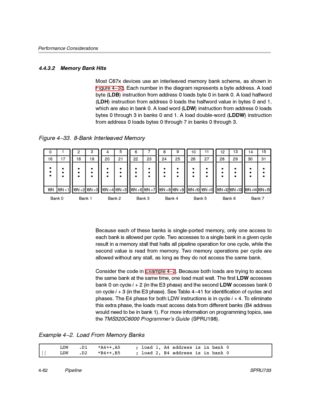
Performance Considerations
Pipeline Stall
Multicycle NOPs
−29. Multicycle NOP in an Execute Packet
Pipeline Phase Branch Target
Cycle #
Data Load
−40. Program Memory Accesses Versus Data Load Accesses
Memory Considerations
Operation
−32. Program and Data Memory Stalls
+10
−33 -Bank Interleaved Memory
Example 4−2. Load From Memory Banks
−41. Loads in Pipeline from Example 4−2
−34 -Bank Interleaved Memory With Two Memory Spaces
Interrupts
Types of Interrupts and Signals Used
Overview
−1. Interrupt Priorities
Priority Interrupt Name Interrupt Type
Nonmaskable Interrupt NMI
Interrupt Acknowledgment Iack and Interrupt Number INUMn
Interrupt Service Table IST
−1. Interrupt Service Table
−2. Interrupt Service Fetch Packet
1238h
Example 5−1. Relocation of Interrupt Service Table
Interrupt Service Table Pointer Istp
−2. Interrupt Control Registers
Summary of Interrupt Control Registers
Acronym Register Name Description
Globally Enabling and Disabling Interrupts
MVC CSR,B0
Individual Interrupt Control
Enabling and Disabling Interrupts
Setting and Clearing Interrupts
Status of Interrupts
Example 5−8. Code to Return From NMI
Returning From Interrupt Servicing
Example 5−9. Code to Return from a Maskable Interrupt
Conditions for Processing a Nonreset Interrupt
Setting the Nonreset Interrupt Flag
Interrupt Detection and Processing
Isfp
Actions Taken During Nonreset Interrupt Processing
Setting the Reset Interrupt Flag
PS PW PR DP DC
Actions Taken During Reset Interrupt Processing
General Performance
Pipeline Interaction
Programming Considerations
Single Assignment Programming
Example 5−11. Code Using Single Assignment
Nested Interrupts
STW
Manual Interrupt Processing
Example 5−14. Manual Interrupt Processing
Example 5−15. Code Sequence to Invoke a Trap
Traps
Example 5−16. Code Sequence for Trap Return
Instruction Compatibility
Instruction C62x DSP C64x DSP C67x DSP C67x+ DSP
Cmpltu
Intsp
Mpylh
Rsqrdp
Subab
Table B−1. Functional Unit to Instruction Mapping
Functional Unit Instruction
Displacement Register
Intdp Intdpu Intsp Intspu
N n n n n n n n n n n n n
STB memory
SUB Subab Subah Subaw Subc Subdp Subsp Subu SUB2 XOR Zero
Unit Instructions and Opcode Maps
Instructions Executing in the .D Functional Unit
Table C−1. Instructions Executing in the .D Functional Unit
Opcode Map Symbols and Meanings
Table C−2. .D Unit Opcode Map Symbol Definitions
Table C−3. Address Generator Options for Load/Store
Syntax Modification Performed
32-Bit Opcode Maps
Figure C−1 or 2 Sources Instruction Format
Appendix D
Instructions Executing in the .L Functional Unit
Table D−1. Instructions Executing in the .L Functional Unit
Table D−2. .L Unit Opcode Map Symbol Definitions
Figure D−1 or 2 Sources Instruction Format
Appendix E
Instructions Executing in the .M Functional Unit
Table E−1. Instructions Executing in the .M Functional Unit
Table E−2. .M Unit Opcode Map Symbol Definitions
Figure E−1. Extended M-Unit with Compound Operations
Appendix F
Instructions Executing in the .S Functional Unit
Table F−1. Instructions Executing in the .S Functional Unit
Table F−2. .S Unit Opcode Map Symbol Definitions
Figure F−1 or 2 Sources Instruction Format
Figure F−7. Branch with NOP Constant Instruction Format
No Unit Specified Instructions and Opcode Maps
Instructions Executing With No Unit Specified
Table G−1. Instructions Executing With No Unit Specified
Figure G−1. Loop Buffer Instruction Format
Index
Cmpeqdp
Dpsp
Index-4
Reset
Index-6
Mpysu
Unit No unit instructions
Rsqrdp
To memory with a 15-bit unsigned constant offset STB
260 Single-precision Subsp 263