MSP50C614 Mixed-Signal Processor Users Guide
Important Notice
About This Manual
How to Use This Manual
Notational Conventions
This document uses the following conventions
Csr ±a /user/ti/simuboard/utilities
This provides three choices *, *+, or *±
Notational Conventions
Trademarks
Information About Cautions and Warnings
This book may contain cautions and warnings
Information About Cautions and Warnings
Page
Contents
Contents
Assembly Language Instructions
Code Development Tools
Contentsix
ROM Usage With Respect to Various Synthesis Algorithms
Applications
Customer Information
Contentsxi
Figures
±11
±10
±12
±13
Tables
±33
±32
±34
±35
Page
Introduction to the MSP50C614
Features of the C614
Features of the C614
Applications
Applications
Introduction to the MSP50C614
Development Device MSP50P614
Development Device MSP50P614
Functional Description
Functional Description
C605 and C604 Preliminary Information
C605 and C604 Preliminary Information
±1. Functional Block Diagram for the C614
Resistor Trim Operation Connections
Crystal Oscillator Operation Connections
±3. Reset Circuit
Terminal Assignments and Signal Descriptions
±1. Signal and Pad Descriptions for the C614
Terminal Assignments and Signal Descriptions
Description Pin #
±2. MSP50C614 100-Pin PJM Plastic Package Pinout Description
PD0 PD1 PD2 PD3 PD4 PD5 PD6
±5 Pin Grid Array Package for the Development Device, P614
VPP VSS VDD DAC M DAC P
MSP50C614 Architecture
Architecture Overview
MSP50C614 Architecture
±1. MSP50C614 Core Processor Block Diagram
ALU
Multiplier
Computation Unit
±1. Signed and Unsigned Integer Representation
Computation Unit
Computation Unit
Arithmetic Logic Unit
±3. Overview of the Multiplier Unit Operation
Accumulator Block
±4. Overview of the Arithmetic Logic Unit
AC0 . . . AC31
Accumulator Block
Accumulator Block Pointers
AP0 . . . AP3
Data Memory Address Unit
Data Memory Address Unit
±6. Data Memory Address Unit
RAM Configuration
Data Memory Addressing Modes
Program Counter Unit
Bit Logic Unit
Program Counter Unit
Memory Organization RAM and ROM
Memory Map
Memory Organization RAM and ROM
Peripheral Communications Ports
±7. C614 Memory Map not drawn to scale
±2. Summary of C614s Peripheral Communications Ports
Reset LOW
Interrupt Name ROM address Event Source Interrupt Priority
Interrupt Vectors
ROM Code Security
Write only
Block Protection Word
Protection marker
= the value programmed at TM5… TM0 true
≡ the binary complement of NTM
= the value programmed at FM5… FM0 false
Interrupt Logic
Macro Call Vectors
Interrupt Logic
IFR
Interrupt Logic
±8. Interrupt Initialization Sequence
Timer Registers
Timer Registers
Triggers INT1 on underflow
Timer Registers
Oscillator Options
Clock Control
PLL Performance
Clock Control
Clock Speed Control Register
±9. PLL Performance
ClkSpdCtrl register
CPU
RTO Oscillator Trim Adjustment
Rtrim Register Read Only Applies to MSP50C614 Device Only
ClkSpdCtrl Value Copied Shaded
Execution Timing
Execution Timing
Reduced Power Modes
Reduced Power Modes
Reduced Power Modes
Reduced Power Modes
Light MID Deep
±3. Programmable Bits Needed to Control Reduced Power Modes
→ deeper sleep … relatively less power →
Component Determined
By Controls
Deeper sleep … Relatively less power → Event Determined
Global interrupt enable is SET
Peripheral Functions
I/O
General-Purpose I/O Ports
Port a Port B Port C Port D Port E
Peripheral Functions
Input Port F
Dedicated Input Port F
Totem-Pole Output Port G
Dedicated Output Port G
Internal and External Interrupts
Branch on D Port
Interrupt Vector Source Trigger Event Priority Comment
±1. Interrupts
Pulse-Density Modulation Rate
Digital-to-Analog Converter DAC
DAC Control and Data Registers
Digital-to-Analog Converter DAC
Overflow bits Least-significant data value Ignored bits
±1. PDM Clock Divider
PDM Clock Divider
Digital-to-Analog Converter DAC
CPU
Pllm
Comparator
TIMER1 starts counting
For INT7 is enabled
Cleared. Refer to .7, Interrupt Logic, for more details
Address
Comparator
Interrupt/General Control Register
Interrupt/General Control Register
IntGenCtrl register
Interrupt/General Control Register
Hardware Initialization States
Hardware Initialization States
Hardware Initialization States
RZF
Bit Bit Name Initialized Value Description
Page
Assembly Language Instructions
System Registers
Introduction
Assembly Language Instructions
Top of Stack, TOS
System Registers
Product High Register PH
Product Low Register PL
Accumulators AC0±AC31
Accumulator Pointers AP0±AP3
Indirect Register R0±R7
Bit
Status Register Stat
String Register STR
Function
±1. Status Register Stat
1 MSP50P614/MSP50C614 Instruction Syntax
Instruction Syntax and Addressing Modes
Addressing Modes
±2. Addressing Mode Encoding
Opcode
Next a
±3. Rx Bit Description
±4. Addressing Mode Bits and adrs Field Description
±6. Auto Increment and Auto Decrement Modes
±5. MSP50P614/MSP50C614 Addressing Modes Summary
Flag Repeat
Flag addressing mode encoding, flagadrs
Flagadrs
Clocks Words Addressing Operation, ² Syntax
Immediate Addressing
Syntax
Example
Direct Addressing
MOV *0x012F * 2, *A0
Mulr *0x02A1
Indirect Addressing
±9. Indirect Addressing Syntax
SyntaxOperation
MOV A2, *R0
Relative Addressing
*R4++
Movb *R7++, A3
Short Relative
A0, *R3+R5
Long Relative
MOV A3, *R6+0x10
TF1, *0x20
Flag Addressing
Or TF2, *R6+0x02
XOR TF1, *R6+0x20
8 Tag/Flag Bits
TF1,*ram1 TF1 bit in Stat is set!?
Possible sources of confusion Consider the following code
Symbol Explanation
±10. Symbols and Explanation
Instruction Classification
Instruction Classification
±11. Symbols and Explanation
±11. Instruction Classification
Class Sub- Description
Class Sub Description
Class 1 Instructions Memory and Accumulator Reference
±12. Classes and Opcode Definition
±14. Class 1a Instruction Description
±13. Class 1 Instruction Encoding
C1a ~A~
C1b
C1b Mnemonic Description
±15. Class 1b Instruction Description
Shltpls a n, adrs
Class 2 Instructions Accumulator and Constant Reference
±16. Class 2 Instruction Encoding
±17. Class 2a Instruction Description
C2a Mnemonic Description
Class 3 Instruction Accumulator Reference
±18. Class 2b Instruction Description
C2b Mnemonic Description
ADD An ~, An ~, imm16 , next a
±19. Class 3 Instruction Encoding
±20. Class 3 Instruction Description
Mnemonic Description
Zero or be set equal to the sign bit Xsgm dependent
MOV SV, An~ , next a
±21. Class 4a Instruction Encoding
Class 4 Instructions Address Register and Memory Reference
±23. Class 4b Instruction Description
±22. Class 4a Instruction Description
±24. Class 4c Instruction Description
±25. Class 4d Instruction Description
Class 5 Instructions Memory Reference
±26. Class 5 Instruction Encoding
±27. Class 5 Instruction Description
RET²
±28. Class 6a Instruction Encoding
Class 6 Instructions Port and Memory Reference
±29. Class 6a Instruction Description
C6a Mnemonic Description
±30. Class 6b Instruction Description
Class 7 Instructions Program Control
C6b Mnemonic Description
Vector8
±31. Class 7 Instruction Encoding and Description
Jcc
Ccc
±32. Class 8a Instruction Encoding
Class 8 Instructions Logic and Bit
±34. Class 8b Instruction Description
±33. Class 8a Instruction Description
Class 9 Instructions Miscellaneous
C8a Mnemonic Description
±36. Class 9a Instruction Description
±35. Class 9a Instruction Encoding
±37. Class 9b Instruction Description
C9a Mnemonic Description
±38. Class 9c Instruction Description
Bit, Byte, Word and String Addressing
±39. Class 9d Instruction Description
C9c Mnemonic Description
±3. Data Memory Organization and Addressing
±40. Data Memory Address and Data Relationship
Mode Address Used Data Order Rx Post modify ²
Movb A0, *0x0003
MOV A0, *0x0004
Which uses the absolute word memory address
±4. Data Memory Example
Rflag
MSP50P614/MSP50C614 Computational Modes
MSP50P614/MSP50C614 Computational Modes
±41. MSP50P614/MSP50C614 Computational Modes
Computational Setting Resetting Function Mode Instruction
SXM
Example 4.6.1 Sovm
Example 4.6.2 Sovm
Example 4.6.1 SXM
Hardware Loop Instructions
Hardware Loop Instructions
Syntax Operation Limitations
±42. Hardware Loops in MSP50P614/MSP50C614
±43. Initial Processor State for String Instructions
String Instructions
String Instructions
Registers register# = value
Mulapl A0, A0~
±44. Lookup Instructions
Lookup Instructions
Lookup Instructions
Instructions Description Data Transfer
MOV An, adrs SUB An MOV An, *An
Special Filter Instructions
Input/Output Instructions
Input/Output Instructions
Xk±2 Xk+2 Xk±1 xk+1 32 or Yk = Σm =0..N hm⋅xk-m
Special Filter Instructions
STR,N±2
STR,0
0x0104
After FIR/COR execution
Important note about setting the Stat register
Firkcoeffs
Coeffarray Samplebuf address
Coeffarray address FIRK/CORK only Program memory FIRK/CORK
FIR/COR only = 0..N
Coeffarray
Samplebuf Coeffarray is stored
Conditionals
Conditionals
Operands
Symbol Meaning
≤ dma6 ≤ ≤ dma16 ≤
≤ port4 ≤ ≤ port6 ≤
Clk
Adrsn
Dma n
Flg
Offset n
Pma n
Port n
±46. Addressing Mode Bits and adrs Field Description
±45. Auto Increment and Decrement
±47. Flag Addressing Syntax and BIts
Individual Instruction Descriptions
Individual Instruction Descriptions
Execution
14.1 ADD Add word
See Also
Description
Addb
PC PC + Flags Affected
Opcode
Clock , clk Words , w
Adds Add String
Adds A1, A1~, A1
14.4 Bitwise
ANDS, ANDB, OR, ORB, ORS, XOR, XORB, Xors
A3, *R4б
TF2, *0x0020
Src byte PC PC +
Andb Bitwise and Byte
OF, SF, ZF, CF are set accordingly
Clock , clk Word , w
Ands A0, A0~, A0
Ands Bitwise and String
Ands A0, A0~, *R2
Clock, clk Word, w
Save next instruction address PC +
Begloop Begin Loop
Flags Affected None Opcode
Order to loop N times
Call Unconditional Subroutine Call
TOS PC +
TOS
R7 +
NOP
True condition Not true condition
±48. Names for cc
Syntax Alternate Syntax Description
0x2010
CALL, VCALL, RET, Iret
CTF1
Crnbe
Stat flags set by src ± src1 operation
14.10 CMP Compare Two Words
PC = PC + w
CMPB, CMPS, Jcc, Ccc
CMP R0, R5
CMP R2, 0xfe20
Cmpb R3
Cmpb Compare Two Bytes
PC PC + w Flags Affected
Cmps Compare Two Strings
Cmps A1~
Cmps A2, A2~
3n R+2
14.13 COR Correlation Filter Function
Xeven = R xeven + R5
Xeven ++
Sample data. During Cork execution, interrupt is queued
Cork Correlation Filter Function
An, *Rx 3nR+2
Rxeven = Rxeven + R5
Decrement R4 by n 1 or First address after Begloop Else
Endloop End Loop
Argument, it assumes n =1
BEGLOOP, Inte
An~ , next a
Extsgn Sign Extend Word
Copy accumulator sign flag SF to all 16 bits of An~
Dest , mod
Extsgns Sign Extend String
Extsgn
2n R+2
14.18 FIR FIR Filter Function Coefficients in RAM
Assembly Language Instructions 101
Firk
Be even. During Firk execution, interrupts are queued
RPT, FIR, COR, Cork
Assembly Language Instructions 103
Idle Halt Processor
Stop processor clocks
14.21 Input From Port Into Word
INS, OUT, Outs
A2~, 0x3d
IN, OUT, Outs
14.22 INS Input From Port Into String
IM is Stat bit
Intd Interrupt Disable
Stat to
INTE, Iret
Inte Interrupt Enable
Assembly Language Instructions 107
INTD, Iret
R7 R7 ±
Iret Return From Interrupt
See Also RET, CALL, C cc, INTE, Intd Description
Return from interrupt. Pop top of stack to program counter
PC PC +
14.26 Jcc Conditional Jumps
110
If test condition is false, a NOP is executed
JNZ
See Also JMP, CALL, C cc Example
JE 0x2010, R3++R5
JIN1 0x2010, R1±±
Post±modify Rx if specified
14.27 JMP Unconditional Jump
RCF and RZF affected by post±modification of Rx
See Also Jcc, CALL, Ccc Example
14.28 MOV Move Data Word From Source to Destination
Clock, clk Word, w With RPT, clk Class
XSF, XZF are set accordingly
TFn, cc , Rx
STR, imm8
116
With some operand types
Example 4.14.28.10 MOV MR, A3, ±±A
MOVU, MOVT, MOVB, MOVBS, Movs
Example 4.14.28.11 MOV A1~, *A1
Example 4.14.28.12 MOV *0x0200 * 2, R0
Example 4.14.28.15 MOV *0x0200 * 2, R0
Example 4.14.28.13 MOV R1, 0x0200
Transfer R5 to R0 Example
Example 4.14.28.18 MOV *R6 + 8 * 2, DP
Movaph Move With Adding PH
Execution + PH
MOVAPHS, MOVTPH, MOVTPHS, MOVSPH, Movsphs
Execution An + PH
Movaphs Move With Adding PH
Background. See .8 for more details
MOVAPH, MOVTPH, MOVTPHS, MOVSPH, Movsphs
Copy value of unsigned src byte to dest byte
Movb Move Byte From Source to Destination
Movb A0, *R2
Copy data memory byte pointed by R2 to accumulator A0
Movb *R2, A0
Movb A0, 0xf2
Movb R2
TAG bit is set to bit 17 th value
Movbs Move Byte String from Source to Destination
Movbs A2, *0x0200
Movbs *0x0200, A2
Movs Move String from Source to Destination
Movs A2~
Movs A1, A1~
Movs A1~, A1
Assembly Language Instructions 127
Movsph
MOVSPHS, MOVAPH, MOVAPHS, MOVTPH, Movtphs
Movsphs Move String With Subtract From PH
Second word ± PH MR contents of adrs
Details
MOVSPH, MOVAPH, MOVAPHS, MOVTPH, Movtphs
PC PC + w Flags Affected None Opcode
Movt
Available
MOVU, MOV, MOVT, MOVB, MOVBS, Movs
TAG bit is set accordingly UM is set to
Movu Move Data Unsigned
MOV, MOVB, MOVT, MOVBS, Movs
Copy the value pointed by R3 to MR
Assembly Language Instructions 131
MR * src PC PC + w Flags Affected
14.38 MUL Multiply Rounded
Accumulator pointer if specified
MULR, MULAPL, MULSPL, MULSPLS, MULTPL, MULTPLS, Mulapl
Muls Multiply String With No Data Transfer
Length nS+2, where nS is the value in STR register
PH,PL MR * src string
MUL, MULR, MULAPL, MULSPL, MULSPLS, MULTPL, Multpls
PH ,PL MR * src
Mulapl Multiply and Accumulate Result
Background. See .8 for more detail
MULAPLS, MULSPL, MULSPLS, MULTPL, Multpls
Mulapls Multiply String and Accumulate Result
MR * src
MULAPL, MULSPL, MULSPLS, MULTPL, Multpls
Occuring in the background. See .8 for more details
Mulspl Multiply and Subtract PL From Accumulator
MULSPLS, MULTPL, MULTPLS, MULAPL, Mulapls
Syntax Description Mulspl adrs
From dest string
Mulspls Multiply String and Subtract PL From Accumulator
MULSPL, MULTPL, MULTPLS, MULAPL, Mulapls
Syntax Description Mulspls adrs
Multpl Multiply and Transfer PL to Accumulator
Execution PH, PL MR * src PC PC + Flags Affected
Multpls
Stored in An string
MULTPL, MULAPL, MULAPLS, MULSPL, Mulspls
Accumulator
Negac Twos Complement Negation of Accumulator
NEGACS, SUB, SUBB, SUBS, ADD, ADDB, ADDS, NOTAC, Notacs
Example 4.14.46.1 Negac A3~, A3, ±±A
Negacs Twos Complement Negation of Accumulator String
Assembly Language Instructions 141
Dest accumulator string
NEGAC, SUB, SUBB, SUBS, ADD, ADDB, ADDS, NOTAC, Notacs
14.48 NOP No Operation
Execution PC PC +
RPT
NOTACS, AND, ANDB, ANDS, OR, ORB, ORS, XOR, XORB, Xors
Notac Ones Complement Negation of Accumulator
NEGAC, Negacs
Example 4.14.49.1 Notac A3~, A3, ±±A
Accumulator string
Notacs Ones Complement Negation of Accumulator String
Negacs
A3~
14.51 or Bitwise Logical or
TFn bits in Stat register are set accordingly
Accumulator pointers are allowed with some operand types
ORB, ORS, AND, ANDS, XOR, XORS, NOTAC, Notacs
Or A0, *R0++R5
Or TF1, *R6+0x22
Or src
14.52 ORB Bitwise or Byte
Accumulator is affected
OR, ORS, AND, ANDS, XOR, XORS, NOTAC, Notacs
PC + w Flags Affected
14.53 ORS Bitwise or String
OR, ORB, AND, ANDS, XOR, XORS, NOTAC, Notacs
ORS A0, A0~, A0
14.54 OUT
Address is multipled by 4 to get the actual port address
OUTS, IN, INS
Port6 specified in the instruction
Outs Output String to Port
OUT, IN, INS
Port6 , An ~
14.56 RET Return From Subroutine CALL, Ccc
Assembly Language Instructions 151
PC TOS
CALL, i.e., RET followed by a RET should not be allowed
Rflag Reset Memory Flag
Sflag , Stag , Rtag
Example 4.14.57.2 Rflag *R6 +
Resets the fractional mode. Clears FM bit of Stat
Reset Fractional Mode Syntax
14.58 RFM
STAT.FM
Saturation output normal mode
Rovm Reset Overflow Mode
Resets the overflow mode to zero
Stat .OM
Load src to repeat counter
14.60 RPT Repeat Next Instruction
Load imm8 to repeat counter
After execution completes
Stag , Rflag , Sflag
Rtag Reset Tag
Rtag *R6+0x0002
Rtag *R6+0x0003
Assembly Language Instructions 157
14.62 RXM Reset Extended Sign Mode
STAT.XM
SXM
Address flagadrs only accesses the 17 th bit
Sflag Set Memory Flag
Rflag , Stag , Rtag
Mode for signed fractional arithmetic
14.64 SFM Set Fractional Mode
Assembly Language Instructions 159
Set fractional mode. Set FM bit of Stat to
PH , PL
14.65 SHL Shift Left
Accumulator. Use Shlac for this purpose
Shls
Its offset. LSB of result is set to zero
Shlac Shift Left Accumulator
Shift accumulator A1 by one bit to the left
Example 4.14.66.2 Shlac A1~, A1, ±±A
Accumulators in the string
Shlacs Shift Left Accumulator String Individually
Example 4.14.68.1 Shlapl A0, *R4++R5
Shlapl Shift Left with Accumulate
Shlapl A2, *R1++
Example 4.14.68.3 Shlapl A1, A1, ++A
Shlapls Shift Left String With Accumulate
Shift data memory string left, add PL to a n
Shift a n ~ string left, addb PL to a n ~
Shls Shift Left Accumulator String to Product
Assembly Language Instructions 165
Execution PH, PL
An~
Example 4.14.71.1 Shlspl A0, *R4++R5
Shlspl Shift Left With Subtract PL
Shlspl A2, *R1++
Example 4.14.71.3 Shlspl A1, A1, ++A
Bit to the next accumulator
Shlspls Shift Left String With Subtract PL
Shlspl , Shltpl , SHLTPLS, SHLAPL, Shlapls
Syntax Description Shlspls An, adrs
Example 4.14.73.1 Shltpl A0, *R4++R5
Shltpl Shift Left and Transfer PL to Accumulator
Shltpl A2, *R1++
Example 4.14.73.3 Shltpl A1, A1, ++A
Execution PH, PL src SV
Shltpls Shift Left String and Transfer PL to Accumulator
Receives the same data as PH
SHLTPL, SHLAPL, SHLAPLS, SHLSPL, Shlspls
Register
Shrac Shift Accumulator Right
Shift right one bit the accumulator A1
Example 4.14.75.2 Shrac A1~, A1, ++A
Shracs Shift Accumulator String Right
Assembly Language Instructions 171
SHRAC, SHL, SHLS, SHLAPL, SHLAPLS, SHLSPL, SHLSPLS, Shltpl
Shltpls
Output DSP mode
Set Overflow Mode Syntax
Sovm
STAT.OM
Stag
RTAG, RFLAG, Sflag
Stag *0x401
Dest, src , src1 , next a
14.79 SUB Subtract
An ~ , An , adrs , next a
An ~ , An ~ , imm16 , next a
SUB A1, A1~, A1
Example 4.14.79.2 SUB A0, A0, 2, ++A
SUB A3~, A3, *R4Ð
SUB R3, R5
Subtract 0x45 from accumulator A2 byte
Subb Subtract Byte
Subtract 0xF2 from register R3 byte
Syntax Description Subb a n, imm8
Subs Subtract Accumulataor String
Assembly Language Instructions 177
Subs A2, A2, A2~
Subs A2, A2~, A2
Subs A3~, A3~, PH
Sets extended sign mode status register Stat bit 0 to
14.82 SXM Set Extended Sign Mode
Assembly Language Instructions 179
RXM
Push PC + 0x7F00
Vcall Vectored Call
R7 R7 + Flags Affected
See Also RET, IRET, CALL, C cc Example
XOR src For two operands
14.84 XOR Logical XOR
XOR src For three operands
TAG bit is set accordingly Src is flagadrs
XORB, XORS, AND, ANDS, OR, ORS, ORB, NOTAC, Notacs
Example 4.14.84.1 XOR A1, A1, 0x13FF
Example 4.14.84.2 XOR A0, A0, 2, ++A
Assembly Language Instructions 183
Xorb Logical XOR Byte
XOR, XORS, AND, ANDS, OR, ORS, ORB, NOTAC, Notacs
Dest string
Xors Logical XOR String
XOR, XORB, AND, ANDS, OR, ORS, ORB, NOTAC, Notacs
Xors A2, A2~, A2
Assembly Language Instructions 185
Reset the content of accumulator A0 to zero
14.87 ZAC Zero Accumulator
Zacs
Zacs Zero Accumulator String
Reset the content of offset accumulator string A1~ to zero
PC PC + Flags Affected ZF =
Zero the specified accumulator string
Assembly Language Instructions 187
Instruction Set Encoding
Instruction Set Encoding
188
Assembly Language Instructions 189
190
Assembly Language Instructions 191
192
Assembly Language Instructions 193
194
True condition Not true condition
Assembly Language Instructions 195
Instruction Set Summary
An~, An~ , next a
Pma16 , Rmod Assembly Language Instructions 197
An~, imm16 , next a
Rx, R5
~, adrs , next a ±46
Adrs, a n~ , next a ±46
Adrs , *An ±46
An ~, imm16 , next a
Adrs, SV
Assembly Language Instructions 199
Adrs, APn
Adrs, TOS
~ , next a
MR, adrs
~, a n~ , next a
~ , a n~
TFn, flagadrs NR+3 TFn, cc , Rx
An~, An~ , next a NR+3 Assembly Language Instructions 201
An~, An~, pma16
An~, An~, An
~, a n, a n~ , next a
~, a n~
~, a n, a n~
~, a n~, PH
Conditional on RZF=0 and RCF=1 Not condition RZF≠0 or RCF≠1
Conditional on RCF=1 Not condition RCF=0
Conditional on RZF=1 Not condition RZF=0
Conditional on ZF=0 and SF=1 Not condition ZF≠0 or SF≠1
Instruction Set Summay
204Assembly Language Instructions
MC = Pllm value+1 ⋅ 131.07 kHz
206Assembly Language Instructions
Summay
Instruction Set Summay 208Assembly Language Instructions
Code Development Tools
Introduction
MSP50C6xx Software Development Tool
MSP50C6xx Software Development Tool
Code Development Tools
PC Requirements
Requirements
Development Requirements
Requirements
Hardware Installation
Hardware Installation
Software Installation
Software Installation
±5. Setup Window
±6. Exit Setup Dialog
±8. Choose Destination Location Dialog
±9. Select Program Folder Dialog
±10. Copying Files
±11.Setup Complete Dialog
Software Emulator
Open Screen
Software Emulator
±13. Project Menu
Projects
±15. File Menu Options
±16. MSP50P614/MSP50C614 Code Development Windows
Description of Windows
±17. RAM Window
±18. CPU Window
±19. Program Window
±20. Hardware Breakpoint Dialog
±21. Inspect Dialog
Debugging a Program
±23. I/O Ports Window
±24. Debug Menu
Software Emulator
±25. Eprom Programming Dialog
±26. Trace Mode
±27. Init Menu Option
Initializing Chip
Emulator Options
±28. Options Menu
Emulator Online Help System
±30. Windows Menu Options
±31. Context Sensitive Help System
Known Differences, Incompatibilities, Restrictions
Assembler
Assembler DLL
Assembler
Assembler Directives
Examples
~ indicates bitwise complement
#IFDEF
#ELSE see #IF and #IFDEF
#IFNDEF symbol
Example #IFDEF symbol
#ELSE
#ENDIF
Assembler
Linker
Linker
C± ± Compiler
Ierr=LINKMAIN sourcefile,exefile
± ± Compiler
Foreword
Variable Types
External References
Type Name Mnemonic Range Size in Bytes Example
4 C± ± Directives
Defines a replacement string for a given string
Without Arguments
With Arguments
Must be present to terminate a #ifdef or #ifndef directive
See #if directive
Include Files
Initializations
Function Prototypes and Declarations
RAM Usage
String Functions
±1. String Functions
An example of the use of xferconst is
Constant Functions
Comparisons
Implementation Details
This section is C± ± specific
Signed comparison of a and b. a is in A0, b is in A0~
Unsigned comparison of a and b. a is in A0, b is in A0~
Assembly Vector
Function Calls
Division
Stack frame has the following structure
Low Address High Address
Cmmfunc bidonint i1,char *i2 is valid, but
Programming Example
On Call
On RET
Ifteststringm2,0,lgm2,LTSN
Programming Example, C ±± With Assembly Routines
±±±±±±±±±±±±±±±
Addb R7,2
To C function return in cmmreturn
±±±±±±±±±±±±±± OldR5 Return Addr Param R7,R5 Stack data
Param ±±±±±±±±±±±±±±
To ASM function return
External
Provided
Data
Iprtc
Implementation Details
Nop ret Dummy interrupt routines
Implementation Details
Implementation Details
Beware of Stack Corruption
Reported Bugs With Code Development Tool
Beware of Stack Corruption
Page
Applications
Application Circuits
Application Circuits
MSP50P614 only 100 kΩ
MSP50C614/MSP50P614 Initialization Codes
MSP50C614/MSP50P614 Initialization Codes
File init.asm
Begloop
~,TIM2REFOSC + TIM2IMR
Overview
Texas Instruments C614 Synthesis Code
Getting Started
Texas Instruments C614 Synthesis Code
Directory Structure
Running the Program
Spkram.irx
ROM
File Description
Adding Another Module
RAM Usage
Understanding the RAM Map
Modifying Files and Projects
These files may be edited for special purpose code
Memory Overlay
These files should never be edited
Creating a New Project
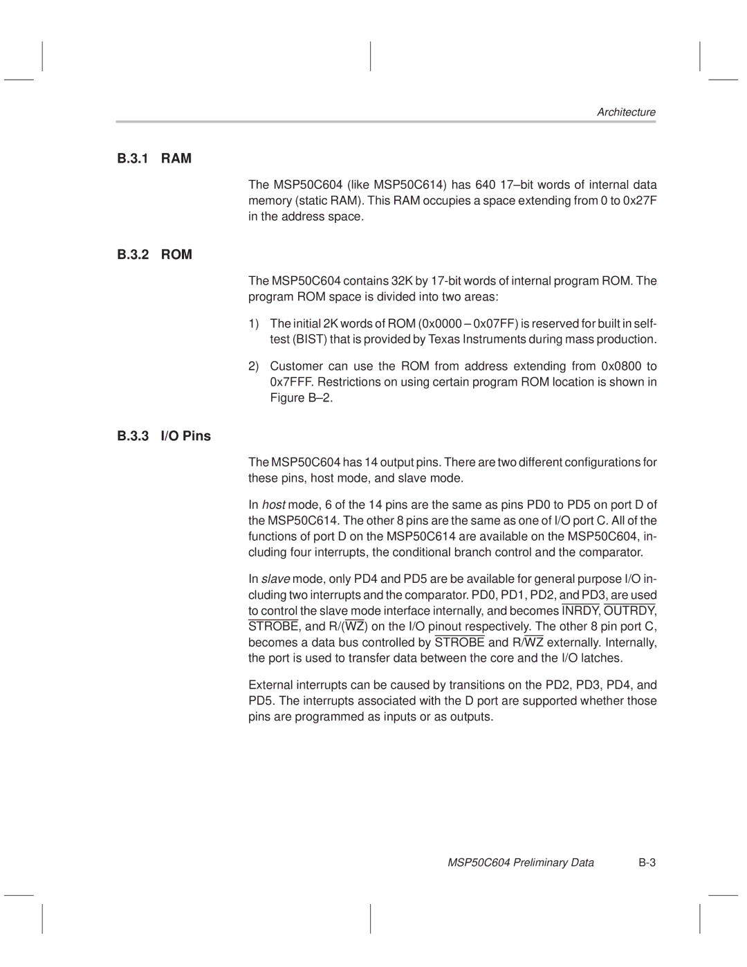
ROM Usage With Respect to Various Synthesis Algorithms
ROM Usage With Respect to Various Synthesis Algorithms
Customer Information
Mechanical Information
Die Bond-Out Coordinates
Mechanical Information
Customer Information
Package Information
±1 -Pin PJM Mechanical Information
±2 -Pin Grid Array Package for the Development Device, P614
±3 Pin Grid Array PGA Package Leads, P614
Customer Information Fields in the ROM
Customer Information Fields in the ROM
Speech Development Cycle
Device Production Sequence
Speech Development Cycle
Nprf
Device Production Sequence
New Product Release Forms
Ordering Information
Ordering Information
614
New Product Release Forms
Authorization to Generate MASKS, PROTOTYPES, and Risk Units
Page
MSP50C605 Preliminary Data
Introduction Features Architecture
Features
Architecture
Port Name IO Location MSP50C614 MSP50C605
1 RAM
3 I/O Pins
2 ROM
Port Description Function Name Address
Figure A±1. MSP50C605 Architecture
Data Memory
Program Memory
Data ROM
Peripheral Ports
Plastic Package
Description Pin#
Page
MSP50C604 Preliminary Data
Introduction Features Architecture Packaging
Introduction
MSP50C604 Preliminary Data
Figure B±1. MSP50C604 Block Diagram
Slave Mode Operation
Host Write Sequence
Host Read Sequence
Program Memory
Data Memory
Peripheral Ports
Interrupts
Packaging
Packaging
Plastic Package
Packaging
Topic
MSP50C605 Data Sheet
MSP50C605 Data Sheet