Data Manual
SM320F2812-HT Contents
Peripherals
SM320F2812-HT
SPI Slave Mode Timing
List of Figures
General-Purpose Input Timing
List of Tables
Interrupt Switching Characteristics
149
Copyright 2009-2010, Texas Instruments Incorporated
Check for Samples SM320F2812-HT
Digital Signal Processor
Supports Extreme Temperature Applications
Description
Introduction
F2812
Hardware Features
Feature
Device Summary
55.0 x 64.0 μm
Die Layout
DIE PAD Backside DIE Size DIE PAD Size
Coordinates Thickness Finish Potential
SM320F2812 172-Pin HFG Cqfp Top View
Pin Assignments
PIN no DIE PAD
Signal Descriptions
Signal Descriptions1
Center Description HFG Xintf Signals
Center Description HFG
Signal Descriptions
Center Description HFG Jtag and Miscellaneous Signals
TDI
Trst
TCK
TMS
Center Description HFG ADC Analog Input Signals
Center Description HFG Power Signals
Gpiob or EVB Signals
SM320F2812-HT
Peripheral PIN no DIE PAD Gpio DIE PAD no
Gpioe or Interrupt Signals
Signal HFG Center
Gpiod or EVA Signals
Gpiod or EVB Signals
Signal HFG Center Gpiof or can Signals
Gpiof or McBSP Signals
Gpiof or XF CPU Output Signal
Signal HFG Center Gpiog or SCI-B Signals
GPIOG4 Scitxdb O
GPIOG5 Scirxdb
Functional Overview
F2812 Memory Map See Notes A. Through G
Memory Map
Address Range Program and Data Space
Addresses of Flash Sectors in F2812
H0 Saram
Wait States
Area
Comments
Peripheral Bus
Brief Descriptions
1 C28x CPU
Memory Bus Harvard Bus Architecture
7 L0, L1, H0 SARAMs
Boot ROM
External Interface Xintf
Flash
Code Security Module Disclaimer
Boot Mode Selection
Boot Mode Selected GPIOF4 GPIOF12 GPIOF3 GPIOF2
Security
Oscillator and PLL
Low-Power Modes
Peripheral Interrupt Expansion PIE Block
External Interrupts XINT1, XINT2, XINT13, Xnmi
Control Peripherals
18 32-Bit CPU Timers 0, 1
Peripheral Frames 0, 1, 2 PFn
General-Purpose Input/Output Gpio Multiplexer
Register Map
Serial Port Peripherals
Name Address Range
Access Type
Peripheral Frame 0 Registers1
Peripheral Frame 1 Registers1
Peripheral Frame 2 Registers1
Device Emulation Registers
External Interface, Xintf
Device Emulation Registers
XZCS7 XWE XRD XR/W Xready XMP/MC Xhold Xholda Xclkout
XZCS0XZCS0AND1 XZCS1
XZCS2
XZCS6 XZCS6AND7
Xrevision Register Bit Definitions
Xintf Configuration and Control Register Mappings
Timing Registers
Xrevision Register
Interrupts
INT1 INT2 INT11 INT12
Intm
CPU PIE Interrupts
11. PIE Configuration and Control Registers1
12. External Interrupts Registers
External Interrupts
System Control
Clock and Reset Domains
13. PLL, Clocking, Watchdog, and Low-Power Mode Registers1
14. Pllcr Register Bit Definitions
OSC and PLL Block
External Reference Oscillator Clock Option
PLL Mode Remarks Sysclkout
Loss of Input Clock
PLL-Based Clock Module
Watchdog Block
Oscclk Clkin Sysclkout
Low-Power Modes Block
16. F2812 Low-Power Modes
Mode
Pschpsc TCR.4
32-Bit CPU-Timers 0/1/2
Tddrhtddr
Prdhprd
INT13 PIE TINT1 TINT0 CPU-TIMER
INT1 to INT12 C28x
INT14 XINT13 TINT2
CPU-Timers 0, 1, 2 Configuration and Control Registers
Module and Signal Names for EVA and EVB
Event Manager Modules EVA EVB Signal
Event Manager Modules EVA, EVB
EVA Registers1
Event Manager a Functional Block Diagram See Note a
Programmable Deadband Generator
General-Purpose GP Timers
Double Update PWM Mode
Full-Compare Units
External ADC Start-of-Conversion
PWM Characteristics
Capture Unit
Quadrature-Encoder Pulse QEP Circuit
Enhanced Analog-to-Digital Converter ADC Module
ADC
Adcenclk Hspclk
MUX ADCINA0
ADCINA7
Adcbgrefin ²
ADCINA70
ADCINB70
Adclo
SM320F2812-HT
Adclo Adcbgrefin
Avddrefbg Avssrefbg
ADC Registers1
Enhanced Controller Area Network eCAN Module
Unit
SN65HVD23x
Can Bus
ECAN Memory Map
Register Name Address
Can Registers Map1
Multichannel Buffered Serial Port McBSP Module
Where Clksrg source could be LSPCLK, CLKX, or CLKR.2
Clkx
TX Fifo
Lspclk
FSX
Data REGISTERS, RECEIVE, Transmit
Name Address Type Reset Value Description
McBSP Register Summary
HEX
Fifo Mode Registers applicable only in Fifo mode
Serial Communications Interface SCI Module
SCI-B Registers1
SCI-A Registers1
−−−−−
10. Serial Communications Interface SCI Module Block Diagram
Serial Peripheral Interface SPI Module
10. SPI Registers1
−−−−−
−−−−−
Register Description
11. Gpio Mux Registers1 2
12. Gpio Data Registers1
PIN
Device and Development Support Tool Nomenclature
Software Development Tools
Hardware Development Tools
Documentation Support
SM320F2812-HT
Value Unit
Absolute Maximum Ratings
Parameter Test Conditions MIN TYP MAX Unit
Electrical Characteristics
Recommended Operating Conditions
MIN NOM MAX Unit
Hours
Die Junction Temperature C
Mode Test Conditions
Vddaio
Current Consumption Graphs
DD Current Reduction mA
Power Sequencing Requirements
Reducing Current Consumption
Peripheral Module
Signal Transition Levels
Recommended Low-Dropout Regulators
Supplier Part Number
Timing Parameter Symbology
VOH 80% 20% VOL
VIH 90% 10% VIL
General Notes on Timing Parameters
Test Load Circuit
85 pF
Clock Table and Nomenclature
Clock Requirements and Characteristics
Device Clock Table
Input Clock Requirements
Possible PLL Configuration Modes1
Output Clock Characteristics
Xclkin Timing Requirements PLL Bypassed or Enabled
Xclkin Timing Requirements PLL Disabled1
Reset XRS Timing Requirements1
Reset Timing
GPIOF14
XF/XPLLDIS
XF/XPLLDIS XMP/MC
Xclkout XRS
XCLKIN/2
Xclkin Xclkout XRS
XCLKIN/8
GPIOF14/XF
Xclkout = Sysclkout
Low-Power Mode Wakeup Timing
10. Idle Mode Switching Characteristics1
A0−A15
11. Standby Mode Switching Characteristics1
Sysclkout Cycles
Device Status Flushing Pipeline Wake−up Signal
Standby
XCLKOUT²
12. Halt Mode Switching Characteristics1
PWM Timing
Event Manager Interface
MAX Unit
13. PWM Switching Characteristics1
14. Timer and Capture Unit Timing Requirements1
Parameter Test Conditions MIN
Interrupt Timing
17. Interrupt Switching Characteristics
TxCTRIP, CxTRIP PDPINTx See Note B
19. General-Purpose Output Switching Characteristics
General-Purpose Input/Output Gpio Output Timing
18. Interrupt Timing Requirements
General-Purpose Input/Output Gpio Input Timing
Qualprd Sysclkout
Qualprd = 1 2 x Sysclkout cycles x Output From Qualifier
SPI Master Mode Timing
21. SPI Master Mode External Timing Clock Phase = 01 2
GPIOxn
Spisomi Master In Data Must Be Valid
Spisimo
22. SPI Master Mode External Timing Clock Phase = 11 2
Spisomi
Data Valid
23. SPI Slave Mode External Timing Clock Phase = 01 2
SPI Slave Mode Timing
SM320F2812-HT
Spisimo Data Must Be Valid
24. SPI Slave Mode External Timing Clock Phase = 11 2
SM320F2812-HT
X2TIMING =
26. Xtiming Register Configuration Restrictions1
External Interface Xintf Timing
27. Valid and Invalid Timing1
28. Xtiming Register Configuration Restrictions1
29. Valid and Invalid Timing when using Synchronous XREADY1
30. Xtiming Register Configuration Restrictions1
32. Asynchronous XREADY1
31. Xtiming Register Configuration Restrictions1
33. Xintf Clock Configurations
Mode Sysclkout Xtimclk Xclkout
XINTCNF2 Clkoff Xtimclk Clkmode
28. Relationship Between Xtimclk and Sysclkout
XR/W
Xintf Signal Alignment to Xclkout
XZCS0AND1, XZCS2 XZCS6AND7
External Interface Read Timing
35. External Memory Interface Read Timing Requirements1
XCLKOUT=XTIMCLK XCLKOUT= 1/2 Xtimclk
Dout
External Interface Write Timing
Lead Active
XCLKOUT=XTIMCLK
SM320F2812-HT
Setup time, Xready Synch low before Xclkout high/low
WS Synch Active Lead Trail
DIN
XREADYSynch
WS Asynch
XCLKOUT=XTIMCLK XCLKOUT= 1/2 Xtimclk XZCS0AND1, XZCS2
XREADYAsynch
Parameter MIN MAX Unit
33. Write With Synchronous Xready Access
34. Write With Asynchronous Xready Access
XWE, XRD XZCS6AND7 XR/W
Xhold and Xholda
XZCS2 XZCS6AND7
XHOLD/XHOLDA Timing
44. XHOLD/XHOLDA Timing Requirements Xclkout = XTIMCLK1 2
XR/W XZCS0AND1
36. XHOLD/XHOLDA Timing Requirements Xclkout = 1/2 Xtimclk
XHOLD/XHOLDA Timing Requirements Xclkout = 1/2 Xtimclk
ADC Absolute Maximum Ratings
On-Chip Analog-to-Digital Converter
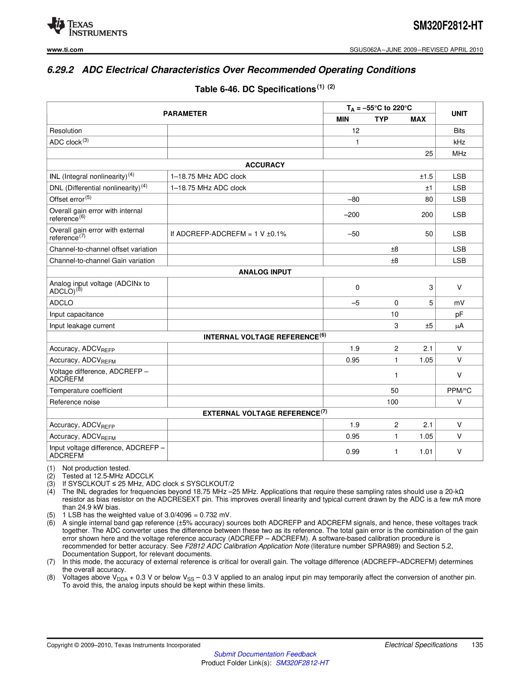
46. DC Specifications1
TYP ADC Operating MODE/CONDITIONS
47. AC Specifications1
48. Current Consumption1
MIN TYP MAX
Pwdnadc
ADC Power-Up Control Bit Timing
ADCIN0
Pwdnbg Pwdnref
Detailed Description
Sequential Sampling Mode Single Channel Smode =
50. Sequential Sampling Mode Timing1
Sample n +
Clock Remarks
AT 25-MHz ADC
Simultaneous Sampling Mode Dual-Channel Smode =
Definitions of Specifications and Terminology
Clkg + Clksrg
Multichannel Buffered Serial Port McBSP Timing
McBSP Transmit and Receive Timing
52. McBSP Timing Requirements1 2
Dxena =
53. McBSP Switching Characteristics1 2
M19
M16 M18
M17 M18
M1, M11 M2, M12 M13
McBSP as SPI Master or Slave Timing
Master Slave Unit MIN MAX
Parameter Master Slave Unit MIN MAX
M39
M49
M58
62. Flash Parameters at 150-MHz SYSCLKOUT1
63. Flash/OTP Access Timing1
Flash Timing
Recommended Operating Conditions
64. Minimum Required Wait-States at Different Frequencies
WAIT-STATE Random Wait STATE2
250
Mechanical Data
Package Type Pins Package Qty Eco Plan Lead
Orderable Device
Samples
Page
Products Applications
DSP
Rfid