RealView Platform Baseboard for ARM926EJ-S
RealView Platform Baseboard for ARM926EJ-S
User Guide
Copyright 2003-2010 ARM Limited. All rights reserved
Product Status
Conformance Notices
RealView Platform Baseboard for ARM926EJ-S User Guide
Chapter Programmer’s Reference
Appendix B Specifications
Appendix G Configuring the USB Debug Connection
List of Tables
Sysmisc
VFP9 implementation 100
Xii
List of Figures
Syssw Sysled
Sysbootcs Sysmisc
Figure D-4 Jtag signal flow on the PCI backplane
Preface
Feedback on
Using this manual
About this manual
Product revision status
Intended audience
Conventions
Typographical
Timing diagrams
Signals
Numbering
Further reading
ARM publications
Xxiii
Other publications
TFT-LCD Module LQ084V1DG21 Sharp Corporation, Osaka, Japan
Feedback
Feedback on this product
Feedback on this manual
Xxvi
Introduction
About the PB926EJ-S
On page 1-3 shows the layout of the PB926EJ-S
PB926EJ-S layout
PB926EJ-S architecture
Time of year clock with backup battery
Field Programmable Gate-Array Fpga that implements
System architecture
Shows the architecture of the PB926EJ-S
2 ARM926EJ-S PXP Development Chip
3 PB926EJ-S Fpga
Displays
RealView Logic Tile expansion
Memory
Clock generators
Debug and test interfaces
Precautions
Ensuring safety
Preventing damage
ARM DUI
Getting Started
Setting up the RealView Platform
Setting the configuration switches
Boot memory configuration
Selecting the boot device
Default switch positions
Switch Default Function in default position
S1-2 S1-1 Device
LED indicators
Lists the PB926EJ-S LED indicators and their function
LED Indicators
Color Device Function
LED ID
Boot Monitor configuration
Connecting Jtag debugging equipment
Jtag connection
USB debug port connection
Connecting the Trace Port Analyzer
Example of MultiTrace and Jtag connection
Example of RealView ICE and RealView Trace
About using trace
Trace connector and adaptor board
Supplying power
Power connectors
Using the PB926EJ-S Boot Monitor and platform library
Running the Boot Monitor
Boot Monitor commands
Lists the commands for the Boot Monitor
Boot Monitor commands
Command Action
Lists the commands for the Debug subsystem
Boot Monitor Configure commands
Boot Monitor Debug commands
Lists the commands for the NOR Flash subsystem
Boot Monitor NOR flash commands
Rebuilding the Boot Monitor
Boot Monitor NOR flash commands CommandAction
Getting Started
Loading Boot Monitor into NOR flash
For RealView DebuggerFrom the Debug menu → Include Commands
Redirecting character output to hardware devices
Rebuilding the platform library
Building an application with the platform library
Loading and running an application from NOR flash
Load region in flash
Using a boot script to run an image automatically
ARM DUI
Fpga on
DMA on
Interrupts on
Hardware Description
ARM926EJ-S PXP Development Chip
1 ARM926EJ-S PXP Development Chip overview
ARM926EJ-S PXP Development Chip block diagram
Embedded Trace Macrocell ETM provides signals for off-chip
This high-performance, low-power Vector Floating-Point VFP
ARM926EJ-S CPU is a member of the ARM9 Thumb family.
ARM926EJ-S r0p3 macrocell is a 32-bit cached processor with
Memory controllers
Configuration control
Synchronous serial port
Configuration switches
Configuration from the DEV Chip Reconfig pushbutton
Configuration signals from SYSCFGDATAx
Restoring the default configuration
AHB bridges and the bus matrix
Simultaneous access
Example of multiple masters
AHB map
Core APB and DMA APB map
Memory interface
Memory devices
AHB monitor
AHB monitor connection
Fpga
Shows the architecture of the Fpga on the PB926EJ-S
Fpga configuration
For details on Fpga components, see
Fpga image 1 this is the image supplied with the board
Localdone Globaldone
Hardware Description
Reset controller
Reset and reconfiguration logic
11 PB926EJ-S reset logic
Reset level
Default values
Memory
Registers Peripherals
12 Reset signal sequence
See -4 on page 3-29 for a description of the reset signals
13 Programmable reset level
Memory aliasing at reset
NSTATICCS1 if one of BOOTCSSEL10 is not b11
14 Boot memory remap logic
Reset signals
Describes reset signals
Reset signal descriptions
Name Function
NPBRESET
NPBSDCRECONFIG
NPLLRESET
NPORESET
Usbwakeup
Reset timing
15 Power-on reset and configuration timing
Power supply control
16 Standby switch and power-supply control
Clock architecture
Clock domains for the PB926EJ-S are shown in Figure
Clock domains for the PB926EJ-S are
ARM926EJ-S PXP Development Chip
Where it can be used as the CPU clock for low-power mode
Signal nGLOBALCLKEN from Z50 on the Logic Tile indicates to
Timing the Ethernet bus. HCLKM2 typically generated from
Controller interface to the Fpga
ARM DUI
1 ARM926EJ-S PXP Development Chip clocks
18 ARM926EJ-S PXP Development Chip internal multiplexors
Lists the clock signals
Default operation
Xtalclkdrv
HCLKM2, HCLKS, PLLCLKEXT, GLOBALCLK,
Xtalclkext
19 Default clock sources and frequencies
Xtalclkext
Example of changing the CPU and bus clock frequencies
Operating the AHB bridges in asynchronous mode
20 Clock sources for asynchronous AHB bridges
HCLKCTRL70
HCLKM1M2F
HCLKM2M2F
HCLKSMF2F
Default value of HCLKCTRL70 is 0xE0
Hclkctrl signal HCLKM1 driven by
Hclkctrl signal HCLKM2 driven by
HCLKM1 selection
Hclkctrl signal Hclks driven by
ICS307 programmable clock generators
Hclks selection
HCLKSL2S and HCLKSL2F from tile
Clcdclkext
Selecting the low-frequency clocks in power-saving mode
Selecting slow start
Peripheral clocks
RealView Logic Tile clocks
10 Globalclk selection
XTALCLK/GLOBALCLK driven by
22 Example of selecting a tile clock for the AHB S bridge
Clock multiplexor logic
23 Clock multiplexors
12 Audio system specification
Characteristic Value
Advanced Audio Codec Interface, Aaci
PCM
No link Passive microphone on CODECMIC1 and CODECMIC2
13 AC’97 audio debug signals on J45
Pin number Signal name Description
Character LCD controller
25 Character display
Clcdc interface
26 Display interface
Chip Reference Manual for interface details
14 Display interface signals
Signal Description
DMA
27 DMA channels
15 DMA signals for external devices
Ethernet interface
USBETHD310
USBETHA82
TPO+ , TPO
About the Smsc LAN91C111
ARM DUI
29 Gpio block diagram
Gpio interface
Interrupts
30 External and internal interrupt sources
Hardware Description
31 KMI block diagram
Keyboard/Mouse Interface, KMI
17 MMC/SD interface signals
Signal Widebus mode SD only MMC mode default
Memory Card Interface, MCI
MMC or SD operation
Card insertion and removal
Card interface description
32 MMI interface
18 MMC signals
MCIPWRx
CARDINx
MCIxDAT30
PCI interface
33 PCI bridge
20 Serial bus signals
Serial bus interface
19 Serial bus addresses Slave address Slave device Bit
Sbscl
Smart Card interface, SCI
35 SCI block diagram
SCIDATAIN0, SCICLKIN0, and SCIDETECT0 signals.
SCICLKINx
NSCICLKENx
SCICLKOUTx
36 SSP block diagram
Synchronous Serial Port, SSP
22 SSP signal descriptions
Name Description
ARM DUI
User switches and LEDs
37 Switch and LED interface
Uart interface
38 UARTs block diagram
NDRVINEN0
SERxTXD
SERxRTS
SERxDTR a
23 Serial interface signal assignment
41 OTG243 block diagram
USB interface
24 USB interface signal assignment
Signal name Direction Description
Test, configuration, and debug interfaces
42 Test and debug connectors, links, and LEDs
Jtag debug normal mode
Jtag and USB debug port support
Jtag configuration mode
Jtag signals
25 Jtag related signals
Name Description Function
25 Jtag related signals Name Description Function
Rtck
Return TCK
NCFGEN
Dbgack
NRTCKEN
43 Jtag connector signals
44 Jtag signal routing
45 RealView Logic Tile Jtag circuitry
ChipScope integrated logic analyzer
Embedded trace support
Ethernet on
MBX on
Timers on
Uart on
Memory map
Sdram
4KB
Memory map
Peripheral Location Interrupt a PIC Address Region SIC Size
Vectored Interrupt Controller PIC
PIC
Uart 0 Interface Dev. chip PIC
PCI
2GB
SIC
ARM Data bus memory map
Configuration and initialization
Remapping of boot memory
Switch is ON, the corresponding Bootcssel signal is High
Removing boot remapping and enabling Sdram at
Enable Sdram at
Simplified version of the remap logic is shown in -14 on
Programmer’s Reference
Booting from NOR flash
Booting from NOR flash
Booting from static expansion memory
Booting from static expansion memory
Booting from AHB expansion memory
Booting from AHB expansion
Memory characteristics
Memory banks
Status and system control registers
Name Address Accessa Reset Description Level
Register map for system control registers
Applycfgword active
Switch Register, Syssw
ID Register, Sysid bit assignment Bits Access Description
ID Register, Sysid
Describes the PB926EJ-S ID Register assignment
LED Register, Sysled
Sysled
Oscillator registers, SYSOSCx
Shows the bit assignment of the registers
Lock Register, Syslock
Describes the PB926EJ-S Lock Register bit assignment
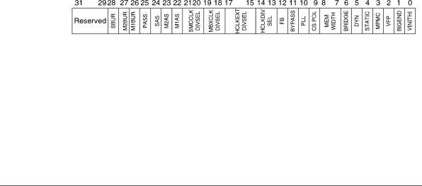
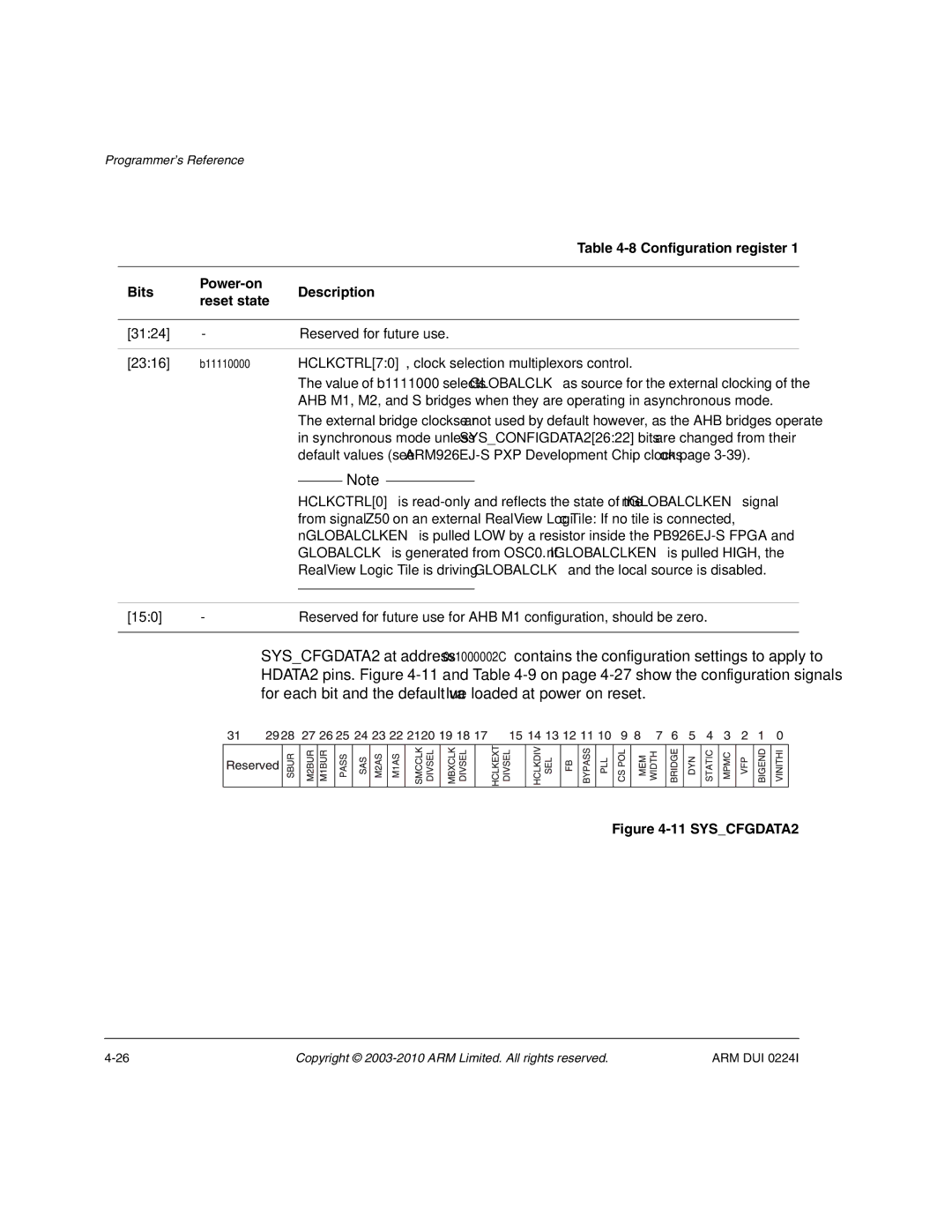
Configuration registers SYSCFGDATAx
6 100Hz Counter, SYS100HZ
Configuration register
Bits Power-on Description Reset state
High
CFGHCLKEXTDIVSEL20, clock control
PLL feedback see ARM926EJ-S PXP Development Chip clocks on
HIGH, then expansion memory is aliased to
Register name Address Access Reset by Description
Flag registers, SYSFLAGx and SYSNVFLAGx
Flag and Nonvolatile Flag Registers
Flag and Nonvolatile Flag Set Registers
Reset Control Register, Sysresetctl
11 Reset level control
Bits Access Description
PCI Control Register, Syspcictl
Flash Control Register, Sysflash
Clcd Control Register, Sysclcd
12 MCI control
13 Flash control
14 Sysclcd
14 Sysclcd register
Boot Select Register, Sysbootcs
14 2.2 inch LCD Control Register Sysclcdser
15 Sysclcdser register
16 Sysbootcs
16 Boot configuration switches
16 24MHz Counter, SYS24MHZ
Miscellaneous System Control Register, Sysmisc
PnINTA LOW
Name Address Access Description
DMA peripheral map registers, SYSDMAPSRx
SYS DMAPSR1
= USB a
Oscillator reset registers, SYSOSCRESETx
19 shows the bit assignment of the registers
20 Oscillator test registers Name Address Access Description
Oscillator test registers, SYSTESTOSCx
AHB monitor
21 AHB monitor implementation
Property Value
DMA
PrimeCell Modifications
22 Aaci implementation
Bit Access Description
23 Modified Aaci PeriphID3 register
Character LCD display
24 Character LCD display implementation
Charcom
Chardat
Charrd
Charmask
An overview of the commands available is listed in Table
26 Character LCD display commands
Command Bit Description Pattern
Color LCD Controller, Clcdc
27 Clcdc implementation
Display resolutions and display memory organization
28 PrimeCell Clcdc register differences
Chip
VGA
Svga 800x600 on Svga 36MHz, 0x2CAC
Epson 2.2in panel Qcif 10MHz, 0x2C2A
Sanyo 3.8in panel Qvga 10MHz, 0x2C2A
320x240
ARM DUI
CLD23
CLD22
CLD21
CLD20
Direct Memory Access Controller and mapping registers
32 Dmac implementation
33 shows the DMA channel allocation
33 DMA channels DMA Requester
21 SYSDMAP0-2 mapping register format
34 DMA mapping register format
Ethernet
35 Ethernet implementation
General Purpose Input/Output, Gpio
36 Gpio implementation
Gpio
Interrupt controllers
37 VIC Primary Interrupt Controller implementation
38 SIC implementation
Fpga
Primary interrupt controller
38 SIC implementation PropertyValue
Dmana
40 Interrupt signals to primary interrupt controller
Bit Interrupt source a Description
VICINTSOURCE31
External interrupt from secondary controller
GND
MBX
Pwrfail
Clcd
Secondary interrupt controller
42 Interrupt signals to secondary interrupt controller
Bit Interrupt Description Source
Handling interrupts
Example 4-1 Clearing and re-enabling SCI0 card out interrupt
Example 4-2 Pseudo code for SIC SCI1 card out interrupt
Example 4-3 Clearing and re-enabling SCI1 card out interrupt
SCI1IMSC SCI1CARDOUTIM
Keyboard and Mouse Interface, KMI
43 KMI implementation
KMI
13 MBX
44 MBX implementation
Move video coprocessor
MultiMedia Card Interfaces, MCIx
45 MCI implementation
MultiPort Memory Controller, Mpmc
Register values
46 Mpmc implementation
47 Sdram register values
Address Register name Value Description Offset
Mpmcclkout runs
SDRAM32M16BRCX32
+0x144 MPMCDynamicRasCas2
PCI controller
48 PCI controller implementation
Dmac
Address Name Access Description
Control registers
PCIIMAPx registers
Map register formats are shown in -25 and -54 on
50 PCI controller registers
Pciselfid register
Pciflags register
Bits Description
52 Pciselfid register format
PCISMAPx registers
PCI configuration
Map register format is shown in -29 and Table
54 PCISMAPx register format
Locating the self-config header table
57 PCI configuration space header
Address Configuration word function Default Offset Value
Configuring the PCI interface
Limitations of the PCI interface
Interrupt Acknowledge Ignored Not available
Real Time Clock, RTC
59 RTC implementation
60 Serial bus implementation Property Value
Sbcontrol
Sbcontrols
Sbcontrolc
Dynamic expansion E2PROM
63 SCI implementation
ARM PrimeCell Synchronous Serial Port Controller PL022
Register, Sysclcd on
Synchronous Static Memory Controller, Ssmc
65 Ssmc implementation
67 Register values for Intel flash, async page mode
Address Name of Ssmc Value Description Register
68 Register values for Samsung Sram
SMBWSTOENR4
SMBWSTWENR4
SMBCR4
SMBWSTBRDR4
System Controller
See also Status and system control registers on
Timers
72 Timer implementation
Uart
73 Uart implementation
PrimeCell Modifications
74 USB implementation
Address Description
Vector Floating Point, VFP9
76 VFP9 implementation
Watchdog
77 Watchdog implementation
102
Signal Descriptions
Signals associated with the SSP are shown in Table A-1
Table A-1 SSP signal assignment
Signal name Description
Synchronous Serial Port interface
Pin Signal Description
Smart Card interface
Table A-3 Signals on expansion connector
Signal Pin Signal name
Table A-4 Serial plug signal assignment
PB926EJ-S provides four serial transceivers
Top Bottom
SER1DTR a SER2DTR a SER3DTR a
Figure A-5 shows the USB connectors
Figure A-6 Audio connectors
Audio Codec interface
MMC and SD flash card interface
Figure A-7 MMC/SD card socket pin numbering
Table A-5 lists the signal assignments
Table A-6 Clcd Interface board connector J18 Pin Signal
Clcd display interface
Clle GND Clac Clcp Cllp Clfp
LCDID0
Clpower
PWR3V5VSWITCH Vlcd Vddposswitch Vddnegswitch
LCDID2
Tsmiso LCDID3 Tsmosi LCDID4 Lcdxwr GND LCDSD0 Lcdxrd Lcdxcs
Figure A-9 Clcd Interface connector J18
Table A-7 VGA connector signals Pin Description
VGA display interface
Figure A-11 Gpio connector
Each data pin has an on-board 10KΩ pullup resistor to
Table A-8 Mouse and keyboard port signal descriptions
Keyboard KMI0, J24 Mouse KMI1, J23 Pin Signal Function
Keyboard and mouse interface
Signals on the Ethernet cable are shown in Table A-9
Table A-9 Ethernet signals Pin Signal
Pin
RealView Logic Tile header connectors
Figure A-14 HDRX, HDRY, and Hdrz upper pin numbering
Hdrx signals
Table A-10 Hdrx J9 signals Platform signal Tile Pin Signal
Table A-10 Hdrx J9 signals
Platform signal Tile Pin Signal
Smcancelwait
HBUSREQM2
HCLKM1DRVL2S
HWRITEM2
HDATAM27
HDATAM28
HDATAM29
HDATAM210
Hdry signals
Table A-11 Hdry J12 signals
Platform signal Tile signal Pin Signal
HRESPS0
Hreadys
Hmastlocks
Hsels
HDATAS5
Ltclcp
HDATAS6
Ltclle
Table A-12 Hdrz J8 signals
Platform signal Tile signal Pin
Hdrz
EXPSMADDR15
EXPSMADDR16
EXPSMADDR17
EXPSMADDR18
Table A-12 Hdrz J8 signals Platform signal Tile signal Pin
Ctdi BOOTCSSEL7 Fpgaimage
Clknegdnin
HCLKM1RESF2L Clkposupout
Dtdoin Dtdoout HCLKSRESF2L Clknegupout
EXPSMDATAS1
EXPSMDATAS2
EXPSMDATAS3
EXPSMDATAS4
EXPSMDATAS26
HBURSTM10
EXPSMDATAS27
HPROTM13
HADDRM119
HDATAM112
HADDRM120
HDATAM111
Figure A-15 Test points and debug connectors
Test and debug connections
Test point Signal Function
This section contains the following subsections
Jtag on page A-36
Overview of test points
SCIDATAOUTTDD0
Intclk
REFCLK1
SPARE2
Jtag
USB debug port
Trace connector pinout
Table A-14 Trace connector J14 Channel Pin
Figure A-18 Embedded logic analyzer connector J33
Figure A-19 AMP Mictor connector
Table A-15 AHB monitor connector J17 Channel Pin
Fpga debug connector pinout
Table A-16 Fpga debug connector J39 Channel Pin
Specifications
Electrical specification
Bus interface characteristics
Table B-1 shows the PB926EJ-S electrical characteristics
Powered from DC
Powered from J34 or PCI bus
Current requirements
Table B-2 Current requirements from DC System Typical Max
Loading on supply voltage rails
Default clock rates for reliable operation are
Clock rate restrictions
HRESETn input
AHB bus timing
Hwrite , HTRANS10 , HSIZE20 , HBURST20 ,
HTRANS10 , HSIZE20 , HBURST20 , and write data
Memory timing
Peripheral timing
Clcdclk
Scirefclk
Sspclk
Mechanical details
Figure B-1 shows the mechanical outline of the PB926EJ-S
ARM DUI
Connectors on page C-15
Clcd Display and Adaptor Board
Figure C-1 Clcd adaptor board connectors bottom view
About the Clcd display and adaptor board
Figure C-2 Small Clcd enclosure
Figure C-3 Large Clcd enclosure
Clcd Display and Adaptor Board
Installing the Clcd display
Figure C-5 Clcd adaptor board connection
Configuration
LCD power control
TDK
CXA-L0612VJL
Switchedvddneg
Switchedfixed Clpower Switchedvddpos
Switchedvddneg
Fixedswitch Invio
Figure C-6 Clcd buffer and power supply control links
Touchscreen controller interface
Touchscreen interface architecture
VBAT21
AUX21
Touch
SSP and Tsci Configuration
Example C-1 SSP to Tsci interface setup
Touchscreen controller programmer’s interface
Example C-2 Configuring and reading the Tsci interface
Connectors
Interface connector
Table C-4 Clcd interface connector J2 Pin Signal
LCD prototyping connector
Table C-5 LCD prototyping connector J1 Signal Pin
Touchscreen prototyping connector
Inverter prototyping connector
5 A/D and keypad connector
Table C-8 A/D and keypad J13 Signal Pin
AUX1 GND AUX2 VBAT1 VBAT2
Mechanical layout
Figure C-9 Clcd adaptor board mechanical layout
ARM DUI
PCI Backplane and Enclosure
Connecting the PB926EJ-S to the PCI enclosure
PCI Backplane and Enclosure
Setting the backplane configuration switches
A socket, the socket is bypassed by an automatic switch
Connecting two PB926EJ-S boards
Figure D-2 Multiple boards on PCI bus
Backplane hardware
Figure D-3 PCI backplane
Table D-1 LED indicators
CLK33ACTIVE
CLK66ACTIVE
CLK133ACTIVE
Table D-2 Configuration switches
Switch Signal Description
Table D-3 Power and reset switches
Test point Signal Description
Figure D-4 Jtag signal flow on the PCI backplane
Power connector
Table D-5 ATX power connector Signal Pin
3V3 12V
NPSON
Logic analyzer connector
Table D-6 Mictor connector pinout
Channel Pin
Jtag connector
Signals on the Jtag connector J5 are shown in Figure D-6
Table D-6 Mictor connector pinout Channel Pin
SPARE4
Memory Expansion Boards
Figure E-1 Dynamic memory board block diagram
About memory expansion
Memory board configuration
Operation without expansion memory
Memory width selection on the static memory board
Table E-1 Memory width encoding
Width
Figure E-3 Memory board installation locations
Fitting a memory board
Eeprom contents
Table E-2 Chip Select information block
Function Address Value Offset
Address Contents Offset
Figure E-4 Chip select information block
EXPnCS memory device string
CS6 access time in 0.1ps LSB
Address Contents Example contents
DYCS3 memory size in bytes
Connector pinout
Expansion connector
DATA0
DATA1
DATA2
DATA3
ADDR0
ADDR1
ADDR2 ADDR3 ADDR4 ADDR5 ADDR6 ADDR7 ADDR8 ADDR9
Table E-6 Static memory connector signals
Pin No Signal
NRAS
NCAS
Table E-6 Static memory connector signals Pin No Signal
Vddio a
ADDR2
NCS4
NCS3
NCS2
ADDR15 NCS0 ADDR16
ADDR17
NIRQ
ADDR18
Figure E-6 Dynamic memory board layout
RealView Logic Tile
About the RealView Logic Tile
Fitting a RealView Logic Tile
Figure F-2 RealView Logic Tile fitted on PB926EJ-S
Header connectors
Variable I/O levels
Figure F-3 HDRX, HDRY, and Hdrz upper pin numbering
RealView Logic Tile I/O
Figure F-4 RealView Logic Tile tristate for I/O
RealView Logic Tile clocks
Table F-1 RealView Logic Tile clock signals
RealView Logic Tile
ARM
AHB buses used by the Fpga and RealView Logic Tiles
AHB M1
AHB S
Example RealView Logic Tile implementation
Figure F-6 Bus signals for RealView Logic Tile and Fpga
Reset
DnTRST pulse
Configuring the USB Debug Connection
Installing the RealView ICE Micro Edition driver
Installing the RealView Developer Suite
Installing the RealView ICE Micro Edition driver on Windows
Select Specify a location
Configuring the USB Debug Connection
Changes to RealView Debugger
Figure G-1 Nodes added to Connection Control window
Using the USB debug port to connect RealView Debugger
Figure G-2 The Connection Control window
Figure G-3 ARM926EJ-S PXP Development Chip detected
Figure G-5 Error shown when no devices are detected
Configuring the USB Debug Connection
Using the Debug tab of the RealView Debugger Register pane
There are three groups of settings
Global Properties
False
True
Jtagclocktype
Device Properties
Semihosting Properties
ARM DUI
Uart Aaci
AHB
Jtag
MCI
Reconfig
DMA KMI
LCD
LED
SYS Resetctl
TCM
Move Uart
SCI
SSP Uart
Xtalclkdrv