Technical Manual
C e m b e r 2 0 0
Trademark Acknowledgment
Audience
Organization
Ansi
Revision Record
PCI Special Interest Group
Conventions Used in This Manual
Revision Date Remarks
ViPreface
Contents
Chapter Signal Descriptions
Chapter Registers
Figures
Contents
Tables
IRDY/, TRDY/, DEVSEL/, STOP/, PERR/, PAR
XivContents
Chapter General Description
Typical LSI53C875A System Application
New Features in the LSI53C875A
Benefits of Ultra Scsi
TolerANT Technology
LSI53C875A Benefits Summary
Scsi Performance
Ease of Use
PCI Performance
Integration
Flexibility
Scripts RAM
Reliability
Testability
Chapter Functional Description
PCI Functional Description
PCI Addressing
PCI Bus Commands and Functions Supported
Configuration Space
Special Cycle Command
PCI Bus Commands and Encoding Types for the LSI53C875A
Interrupt Acknowledge Command
CBE30 Command Type Supported as Master Supported as Slave
Reserved Command
2.3 I/O Read Command
2.4 I/O Write Command
Memory Read Command
Memory Read Line Command
Memory Read Multiple Command
Dual Address Cycle DAC Command
PCI Functional Description
Memory Write and Invalidate Command
PCI Cache Mode
Enabling Cache Mode
Issuing Cache Commands
Memory Read Caching
Memory Write Caching
PCI Cache Mode Alignment
Host Memory
Examples
Read Example
Write Example
Write Example
Scsi Functional Description
Memory-to-Memory Moves
Phase Mismatch Handling in Scripts
Scripts Processor
Internal Scripts RAM
3 64-Bit Addressing in Scripts
Hardware Control of Scsi Activity LED
Using the Scsi Clock Quadrupler
Designing an Ultra Scsi System
Prefetching Scripts Instructions
Opcode Fetch Burst Capability
Load and Store Instructions
Jtag Boundary Scan Testing
Scsi Loopback Mode
Parity Options
Bits Used for Parity Control and Generation
Bit Name Location Description
Scsi Parity Errors and Interrupts
Scsi Parity Control
DMA Fifo
Parity Checking/Generation
DMA Fifo Sections
Data Paths
LSI53C875A Host Interface Scsi Data Paths
Asynchronous Scsi Send
Synchronous Scsi Send
Asynchronous Scsi Receive
Synchronous Scsi Receive
Scsi Bus Interface
Scsi Termination
Select/Reselect During Selection/Reselection
Regulated Termination for Ultra Scsi
Synchronous Operation
Determining the Data Transfer Rate
Determining the Synchronous Transfer Rate
Scsi Transfer Sxfer Register, Bits 75 TP20
Scsi Control Three SCNTL3 Register, Bits 64 SCF20
Scsi Control Three SCNTL3 Register, Bits 20 CCF20
Ultra Scsi Synchronous Data Transfers
Registers
Interrupt Handling
Polling and Hardware Interrupts
Functional Description
Fatal vs. Nonfatal Interrupts
Masking
Stacked Interrupts
Halting in an Orderly Fashion
Sample Interrupt Service Routine
Read Interrupt Status Zero ISTAT0
Chained Block Moves
Block Move and Chained Block Move Instructions
Wide Scsi Send Bit
Sodl Register
Wide Scsi Receive Bit
Swide Register
Chained Block Move Scripts Instruction
Parallel ROM Interface
Parallel ROM Support
MAD31 Available Memory Space
Default Download Mode
Serial Eeprom Interface
Mode a Serial Eeprom Data Format
Power Management
No Download Mode
Byte Name Description
Power States
Power State D0
Power State D1
Configuration Register Bits
Power State D2
Power State D3
Functional Description
Chapter Signal Descriptions
LSI53C875A Functional Signal Grouping
LSI53C875A Functional Signal Grouping
Signal Name Pull-up Current Conditions for Pull-up
Signal Descriptions
Internal Pull-ups on LSI53C875A Signals
LSI53C875A Internal Pull-ups
System Signals
PCI Bus Interface Signals
System Signals
Type Strength Description
Bus Command and Byte Enables are
Address and Data Signals
Address and Data Signals
Initialization Device Select is used as a chip select
Interface Control Signals
Interface Control Signals
Arbitration Signals
Arbitration Signals
Error Reporting Signals
Error Reporting Signals
Scsi Bus Interface Signal
Scsi Bus Interface Signals
Interrupt Signal
Interrupt Signal
Scsi Signals
Scsi Signals
Scsi Control Signals
10 Scsi Control Signals
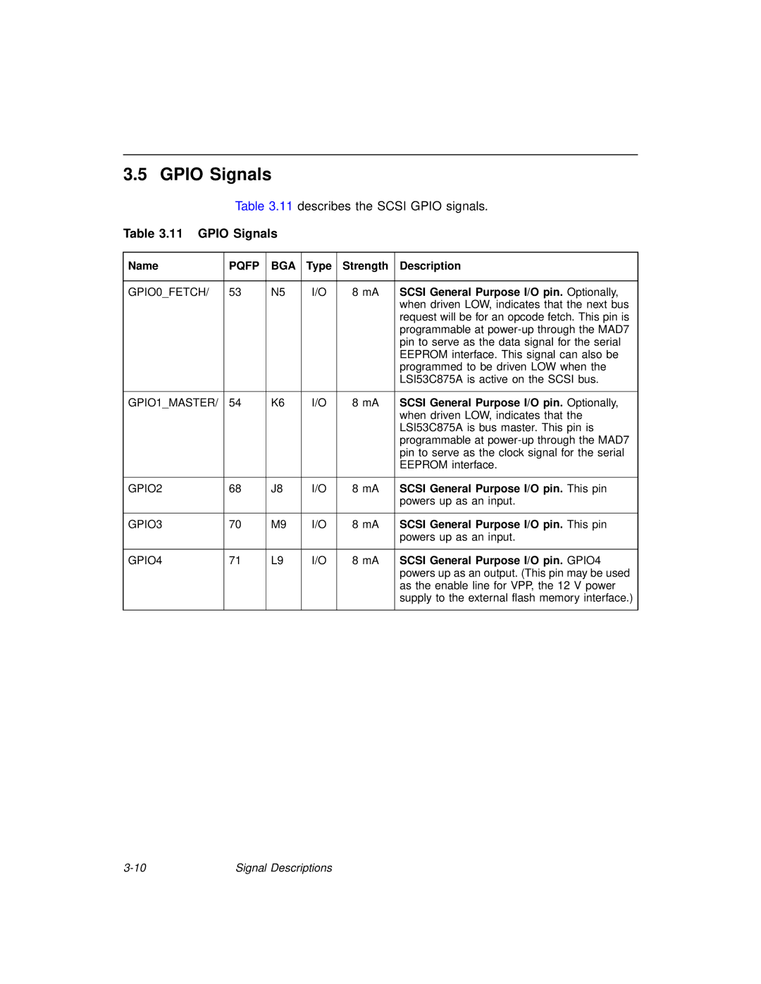
Scsi General Purpose I/O pin. Optionally
Gpio Signals
11 Gpio Signals
Scsi General Purpose I/O pin. This pin
ROM Flash and Memory Interface Signals
12 ROM Flash and Memory Interface Signals
Memory Address/Data Bus. This bus is used
Test Interface Signals
13 Test Interface Signals
Power and Ground Signals
14 Power and Ground Signals
15 Decode of MAD Pins
MAD Bus Programming
MAD Bus Programming
Signal Descriptions
PCI Configuration Registers
Chapter Registers
VIDVendor ID150
Registers
Vendor ID Read Only
Device ID Read Only
Command Read/Write
Enable Parity Error Response
DIDDevice ID150
EMS
WIE
EBM
EIS
RMA
DPE
SSE
RTA
Revision ID Rev ID Read Only
Register
DPR
RIDRevision ID70
Registers 0x09-0x0B
Register 0x0C
Register 0x0F
Register 0x0D
Register 0x0E
BAR0
BAR1
Registers 0x28-0x2B
Registers 0x18-0x1B
Registers 0x1C-0x27
Registers 0x2C-0x2D
SID
Registers 0x2E-0x2F
Subsystem ID Read Only
Subsystem ID 150
Expansion ROM Base Address 310
Expansion ROM Base Address Read/Write
Erba
Capabilities Pointer Read Only CPCapabilities Pointer70
Registers 0x35-0x3B
Register 0x3C
Interrupt Line Read/Write ILInterrupt Line70
Register 0x3F
Register 0x3D
Register 0x3E
MGMINGNT70
Pmes
DSI
D2S
D1S
APS
PEN
Dscl
Dslt
Bridge Support Extensions Pmcsrbse Read Only
DATAData70
Scsi Registers
Data Read Only
Scsi Register Address Map
Scsi Control Zero SCNTL0 Read/Write
ARB10 Arbitration Mode Bits 1
Arbitration Mode
Simple Arbitration
Full Arbitration, Selection/Reselection
Start Start Sequence5
AAP
Watn
EPC
DHP
EXC
ADB
Aesp
CON
RST
Iarb
SSTStart Scsi Transfer0
SDU
Chained Mode
Scsi Control Two SCNTL2 Read/Write
Scsi Disconnect Unexpected
WSS
Slpmd
Slphben
VUE0
Scsi Control Three SCNTL3 Read/Write
Ultra Scsi Enable
WSRWide Scsi Receive0
USE
EWS
Enable Wide Scsi
SCF20 Synchronous Clock Conversion Factor
CCF20 Clock Conversion Factor
ENC
RRE
SRE
Scsi Transfer Sxfer Read/Write
TP20 Scsi Synchronous Transfer Period
Bits Period ns Mbytes/s
Synch CLK MHz
Transfer Rate
MO40 Max Scsi Synchronous Offset
Maximum Synchronous Offset
Synchronous Offset
General Purpose GPREG0 Read/Write
Scsi Destination ID Sdid Read/Write
Encoded Destination Scsi ID
Gpio
Scsi First Byte Received Sfbr Read/Write
Sfbr Scsi First Byte Received70
BSY
REQ
ACK
SEL
VAL
Register 0x0A
Register 0x0B
Enid
SBSY/ Status
SREQ/ Status
SACK/ Status
SSEL/ Status
SSI
Mdpe
Abrt
SIR
Scsi Registers
OLF
ILF
ORF
WOA
AIP
LOA
SSTAT2 bit
Scsi Synchronous Data Fifo Word Count
Bytes or Words
SDP0L
OLF1
ILF1
ORF1
SDP1
SPL1
Ldsc
DSA
Abort Operation
Srst Software Reset6
Interrupt Status Zero ISTAT0 Read/Write
SEM
Signal Process
Sigp
Semaphore
Sipscsi Interrupt Pending1
Dipdma Interrupt Pending0
Syncirqd
Flsh
Srun
Mailbox One MBOX1 Read/Write
Mailbox Zero MBOX0 Read/Write
MBOX0 Mailbox Zero70
MBOX1 Mailbox One70
Chip Test One CTEST1 Read Only
Chip Test Zero CTEST0 Read/Write
FMTByte Empty in DMA FIFO70
FFLByte Full in DMA FIFO70
CIO
Register 0x1A
Ddir
Dack
Teop
Dreq
CLF
Register 0x1B
FLF
DMA Fifo Dfifo
Registers 0x1C-0x1F
Temp
58Registers
ZSD
Bdis
FBL3
Srtm
Adck
FBL20 Fifo Byte Control
Chip Test Five CTEST5 Read/Write
Clock Address Incrementor
Masr
Bbck
DFS
BL2
Dfdma FIFO70
DBC
DMA Command Dcmd Read/Write
Dcmd DMA Command70
DSP
Registers 0x2C-0x2F
Dnad
Scratch Register a Scratcha Read/Write
DMA Scripts Pointer Save Dsps Read/Write
Dsps DMA Scripts Pointer Save310
Scratcha Scratch Register a 310
DMA Mode Dmode Read/Write
BL10 Burst Length
ERLEnable Read Line3
Source I/O Memory Enable
Destination I/O Memory Enable
Siom
Ermp
Enable Read Multiple
Burst Opcode Fetch Enable
BOF
Scripts Interrupt Instruction Received Reserved
DMA Interrupt Enable Dien Read/Write
Master Data Parity Error Bus Fault
Illegal Instruction Detected
Clse
Register 0x3A
Register 0x3B
PFF
Irqmirq Mode3
Single Step Mode
SSM
Irqd
IRQ Disable
STDStart DMA Operation2
COMLSI53C700 Compatibility0
Adder
Registers 0x3C-0x3F
0x40
SGE
CMP
RSL
UDC
STO
GEN
Scsi Interrupt Status Zero SIST0 Read Only
HTHHandshake-to-Handshake Timer Expired0
Initiator Mode Phase Mismatch Target Mode SATN/ Active
This bit is set when an arbitration only or full arbitration
PAR
Parity Error
Scsi RST/ Received
Scsi Interrupt Status One SIST1 Read Only
Scsi Longitudinal Parity Slpar Read/Write
Handshake-to-Handshake Timer Expired
HTH
Slpar Scsi Longitudinal Parity70
Data Bytes Running Slpar
Swide Scsi Wide Residue70
Memory Access Control Macntl Read/Write
Scsi Wide Residue Swide Read/Write
TYP
Pscpt
DWR
DRD
Scpts Scripts
Scsi Timer Zero STIME0 Read/Write
Gpio Enable
Gpiogpio Enable10
HTH30 Handshake-to-HandshakeTimer Period
SEL30 Selection Time-Out30
Hthsf
Hthba
Gensf
Register 0x4A
Register 0x4B
SLT
Register 0x4C
Ssaid
ART
ISO
Register 0x4D
Sclk
QEN
SCE
Register 0x4E
Qsel
ROF
EXT
SZM
AWS
LOW
Register 0x4F
STR
S16 Bit System
Disable Single Initiator Response
Timer Test Mode
TTM
Sidlscsi Input Data Latch150
STW
Scsi Input Data Latch Sidl Read Only
Register 0x53
Lock
Enpmj
Enable Phase Mismatch Jump
Chip Control 0 CCNTL0 Read/Write
Pmjctl Jump Control6
Dils
Enndj
Disfc
64TIMOD
Zmode
Ddac
EN64DBMV
Enable 64-Bit Direct Bmov
EN64TIBMV
Scsi Bus Data Lines Sbdl Read Only
Registers 0x5C-0x5F
64-Bit Scripts Selectors
Register 0x5A-0x5B
Registers 0x60-0x9F
Mmrs
Registers 0xA0-0xA3
Memory Move Read Selector Mmrs Read/Write
Memory Move Read Selector Mmrs
Mmws
Registers 0xA4-0xA7
Registers 0xA8-0xAB
SFS
DRS
Registers 0xAC-0xAF
Registers 0xB0-0xB3
Sbms
Registers 0xB8-0xBB
Phase Mismatch Jump Registers
Registers 0xB4-0xB7
Registers 0xBC-0xBF
PMJAD1
Registers 0xC0-0xC3
Registers 0xC4-0xC7
PMJAD2
RBC
Registers 0xC8-0xCB
Registers 0xCC-0xCF
ESA
Registers 0xD0-0xD3
Entry Storage Address ESA Read/Write
Entry Storage Address 310
SBC
Registers 0xD4-0xD7
Registers 0xD8-0xDA
Registers 0xE0-0xFF
Register 0xDB
Registers 0xDC-0xDF
Csbc
Low Level Register Interface Mode
Scsi Scripts
High Level Scsi Scripts Mode
Instruction Description
Sample Operation
Scripts Instructions
Scsi Scripts Instruction Set
Scripts Overview
Block Move Instruction
First Dword
Table Indirect Bit Addressing
Direct Addressing
TIA
Command Not Used Don’t Care
OPC Instruction Defined
Target Mode
OPCOpCode27
Initiator Mode
SCSIP20 Scsi Phase2624
TC230 Transfer Counter230
Scsi Information Transfer Phase
Scsi Phase
Second Dword
Target Mode Initiator Mode
I/O Instruction
Start Address 310
Reselect Instruction
IT10 Instruction Type I/O Instruction 3130
OPC20 OpCode 2927
Instruction Defined
Set Instruction
Disconnect Instruction
Wait Select Instruction
Clear Instruction
Select Instruction
Wait Disconnect Instruction
Wait Reselect Instruction
Relative Addressing Mode
TITable Indirect Mode25
Relative
Direct
Table Indirect
Bit
Command Table Offset Absolute Jump Offset
Table Relative
Set/Clear Sack Reserved
Set/Clear Satn
O20 Operator 2624
Read/Write Instructions
IT10 Instruction Type Read/Write Instruction 3130
Use data8/SFBR
Read-Modify-Write Cycles
A60 Register Address A60 2216
Move To/From Sfbr Cycles
Read/Write Instructions
Transfer Control Instructions
Jump Instruction
IT10 Instruction Type Transfer Control 3130
Transfer Control Instructions
Call Instruction
Return Instruction
Interrupt Instruction
Interrupt-on-the-Fly Instruction
Jump/Call an Absolute Address
Scsi Phase Comparisons
RARelative Addressing Mode23
Jump/Call a Relative Address
Jump If True/False
Bit 2 is asserted
JMP
Compare Data
Compare Phase
Wait for Valid Phase
WVP
Data Compare Value
Memory Move Instructions
DCV
Jump Address 310
No Flush
IT20 Instruction Type Memory Move 3129
Reserved 2825
Read/Write System Memory from Scripts
Dsps Register 310
Temp Register 310
Load and Store Instructions
Third Dword
Bit A1 Bit A0 Number of Bytes Allowed to Load and Store
Reserved 2726 No Flush Store instruction only
IT20 Instruction Type 3129
DSA Relative
Bit Source Destination
This bit has no effect unless the Prefetch Enable bit
DMA Control Dcntl register is set
Scsi Scripts Instruction Set
Chapter Electrical Specifications
DC Characteristics
Operating Conditions1
Symbol Parameter Min Max Unit Test Conditions
Absolute Maximum Stress Ratings1
Input Capacitance
Bidirectional Signals-MAD70, MAS/10, MCE/, MOE/, MWE
Bidirectional Signals-GPIO0FETCH/, GPIO1MASTER/, GPIO24
Output Signal-TDO
Output Signal-SERR
TolerANT Technology Electrical Characteristics
Output Signals-IRQ/, MAC/TESTOUT, REQ
Symbol Parameter Min1 Max Unit Test Conditions
Pqfp
Rise and Fall Time Test Condition
Input Current as a Function of Input Voltage
12 External Clock1
AC Characteristics
Symbol Parameter Min Max Unit
Reset Input
Interrupt Output
PCI and External Memory Interface Timing Diagrams
Electrical Specifications
Target Timing
15 PCI Configuration Register Read
PCI Configuration Register Read
16 PCI Configuration Register Write
10 PCI Configuration Register Write
17 32-Bit Operating Register/SCRIPTS RAM Read
11 32-Bit Operating Register/SCRIPTS RAM Read
18 64-Bit Address Operating Register/SCRIPTS RAM Read
12 64-Bit Address Operating Register/SCRIPTS RAM Read
19 32-Bit Operating Register/SCRIPTS RAM Write
13 32-Bit Operating Register/SCRIPTS RAM Write
20 64-Bit Address Operating Register/SCRIPTS RAM Write
14 64-Bit Address Operating Register/SCRIPTS RAM Write
Initiator Timing
21 Nonburst Opcode Fetch, 32-Bit Address and Data
15 Nonburst Opcode Fetch, 32-Bit Address and Data
22 Burst Opcode Fetch, 32-Bit Address and Data
16 Burst Opcode Fetch, 32-Bit Address and Data
23 Back-to-Back Read, 32-Bit Address and Data
17 Back-to-Back Read, 32-Bit Address and Data
24 Back-to-Back Write, 32-Bit Address and Data
18 Back-to-Back Write, 32-Bit Address and Data
25 Burst Read, 32-Bit Address and Data
19 Burst Read, 32-Bit Address and Data
26 Burst Read, 64-Bit Address and Data
20 Burst Read, 64-Bit Address and Data
27 Burst Write, 32-Bit Address and Data
21 Burst Write, 32-Bit Address and Data
28 Burst Write, 64-Bit Address and 32-Bit Data
22 Burst Write, 64-Bit Address and 32-Bit Data
External Memory Timing
29 External Memory Read
23 External Memory Read
STOP/ Driven by LSI53C875A
30 External Memory Write
External Memory Write timings start on
24 External Memory Write
Data Byte Enable
Address out from MOE/, MCE/ High
Driven by LSI53C875A Higher Valid Write Data
CBE30 Byte Enable
Data Byte Enable Out Lower Address
Data LSI53C875A-Data
Data Byte Enable Data Out
Symbol Parameter Min
Slow Memory ≤ 128 Kbytes Read Cycle
Slow Memory ≤ 128 Kbytes Write Cycle
30 Slow Memory ≤ 128 Kbytes Write Cycle
≤ 64 Kbytes ROM Read Cycle
≤ 64 Kbyte ROM Write Cycle
32 ≤ 64 Kbyte ROM Write Cycle
Scsi Timing Diagrams
37 Initiator Asynchronous Send
38 Initiator Asynchronous Receive
34 Initiator Asynchronous Receive
39 Target Asynchronous Send
35 Target Asynchronous Send
40 Target Asynchronous Receive
41 SCSI-1 Transfers 5.0 Mbytes
Symbol Parameter Min Max Unit
37 Initiator and Target Synchronous Transfer
Package Diagrams
38 LSI53C875A 160-Pin Pqfp Mechanical Drawing
Pin Pqfp P3 Mechanical Drawing Sheet 2
Signal Pin
44 160 Pqfp Pin List by Location
Pin BGA Mechanical Drawing
45 169 BGA Pin List by Location
NC1
Appendix a Register Summary
Table A.2 LSI53C875A Scsi Register Map
Register Summary
Scratch Registers C-RSCRATCHC-SCRATCHR
Table A.2 LSI53C875A Scsi Register Map
Register Summary
Appendix B External Memory Interface Diagram Examples
Figure B.2 64 Kbyte Interface with 150 ns Memory
External Memory Interface Diagram Examples
Figure B.4 512 Kbyte Interface with 150 ns Memory
Symbols
Index
IX-2Index
Numerics
SGE 4-74,4-77 SI
IX-4Index
IX-5
IX-6Index
IX-7
IX-8Index
IX-9
IX-10Index
Customer Feedback
Reader’s Comments
Excellent Good Average Fair Poor
Distributors by State
California
New York
Direct Sales Representatives by State Component and HAB
Sales Offices and Design Resource Centers
North America
Korea
International Distributors
Australia Hong Kong