MDIO Registers | www.ti.com |
4 MDIO Registers
4.1Introduction
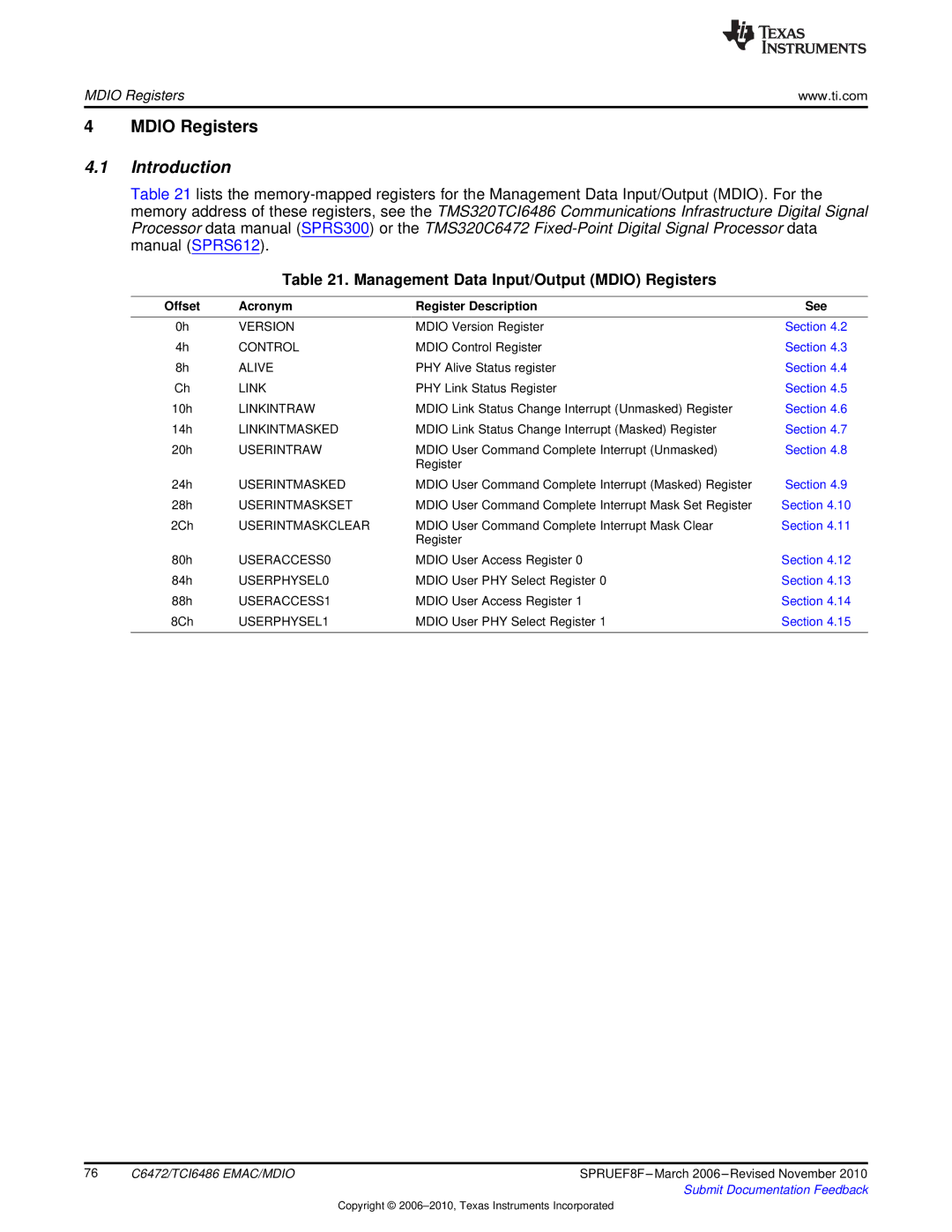
Table 21 lists the
Table 21. Management Data Input/Output (MDIO) Registers
Offset | Acronym | Register Description | See |
0h | VERSION | MDIO Version Register | Section 4.2 |
4h | CONTROL | MDIO Control Register | Section 4.3 |
8h | ALIVE | PHY Alive Status register | Section 4.4 |
Ch | LINK | PHY Link Status Register | Section 4.5 |
10h | LINKINTRAW | MDIO Link Status Change Interrupt (Unmasked) Register | Section 4.6 |
14h | LINKINTMASKED | MDIO Link Status Change Interrupt (Masked) Register | Section 4.7 |
20h | USERINTRAW | MDIO User Command Complete Interrupt (Unmasked) | Section 4.8 |
|
| Register |
|
24h | USERINTMASKED | MDIO User Command Complete Interrupt (Masked) Register | Section 4.9 |
28h | USERINTMASKSET | MDIO User Command Complete Interrupt Mask Set Register | Section 4.10 |
2Ch | USERINTMASKCLEAR | MDIO User Command Complete Interrupt Mask Clear | Section 4.11 |
|
| Register |
|
80h | USERACCESS0 | MDIO User Access Register 0 | Section 4.12 |
84h | USERPHYSEL0 | MDIO User PHY Select Register 0 | Section 4.13 |
88h | USERACCESS1 | MDIO User Access Register 1 | Section 4.14 |
8Ch | USERPHYSEL1 | MDIO User PHY Select Register 1 | Section 4.15 |
|
|
|
|
76 | C6472/TCI6486 EMAC/MDIO | SPRUEF8F |
|
| Submit Documentation Feedback |
Copyright ©
