EMAC Functional Architecture | www.ti.com |
Table 10. EMAC and MDIO Signals for RGMII Interface (continued)
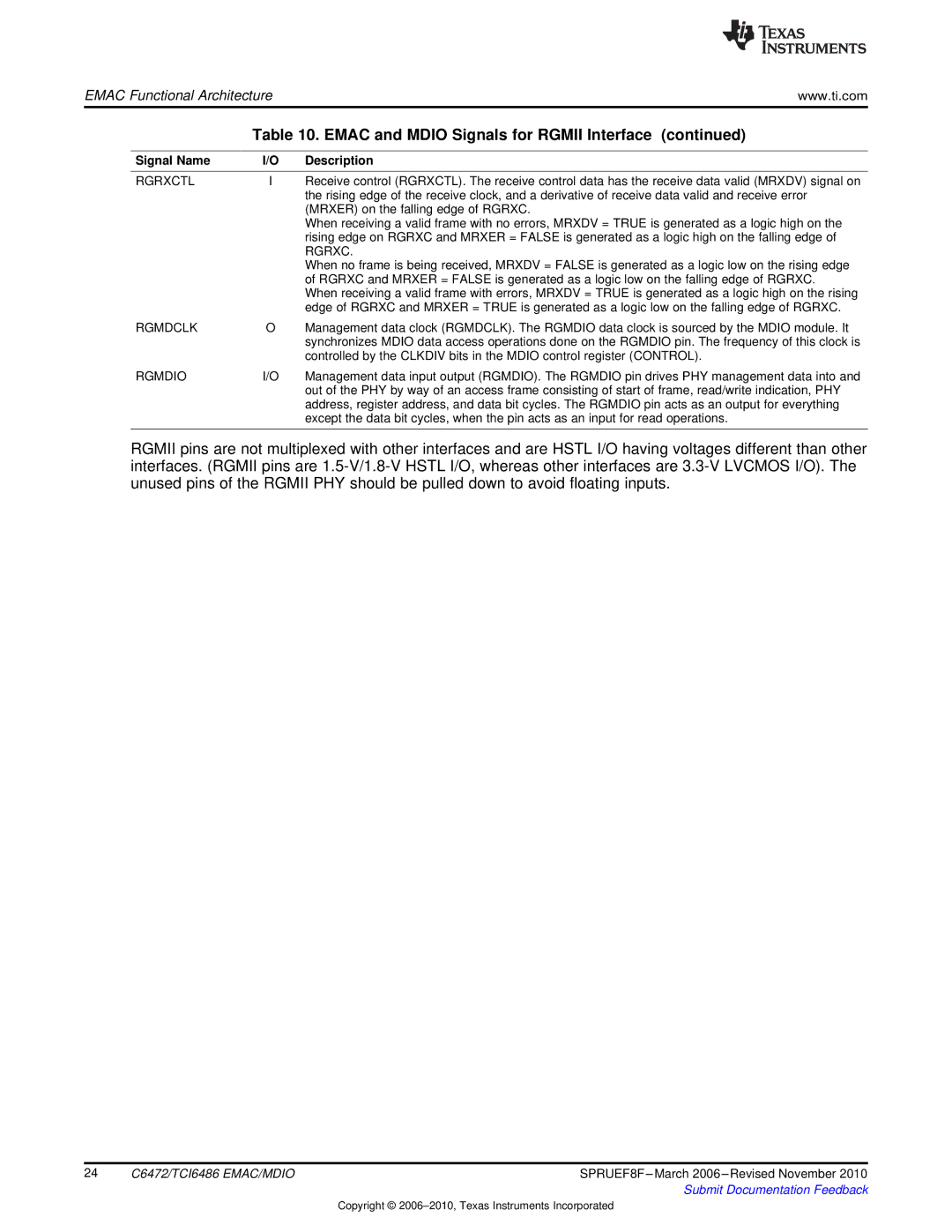
Signal Name | I/O | Description |
RGRXCTL | I | Receive control (RGRXCTL). The receive control data has the receive data valid (MRXDV) signal on |
|
| the rising edge of the receive clock, and a derivative of receive data valid and receive error |
|
| (MRXER) on the falling edge of RGRXC. |
|
| When receiving a valid frame with no errors, MRXDV = TRUE is generated as a logic high on the |
|
| rising edge on RGRXC and MRXER = FALSE is generated as a logic high on the falling edge of |
|
| RGRXC. |
|
| When no frame is being received, MRXDV = FALSE is generated as a logic low on the rising edge |
|
| of RGRXC and MRXER = FALSE is generated as a logic low on the falling edge of RGRXC. |
|
| When receiving a valid frame with errors, MRXDV = TRUE is generated as a logic high on the rising |
|
| edge of RGRXC and MRXER = TRUE is generated as a logic low on the falling edge of RGRXC. |
RGMDCLK | O | Management data clock (RGMDCLK). The RGMDIO data clock is sourced by the MDIO module. It |
|
| synchronizes MDIO data access operations done on the RGMDIO pin. The frequency of this clock is |
|
| controlled by the CLKDIV bits in the MDIO control register (CONTROL). |
RGMDIO | I/O | Management data input output (RGMDIO). The RGMDIO pin drives PHY management data into and |
|
| out of the PHY by way of an access frame consisting of start of frame, read/write indication, PHY |
|
| address, register address, and data bit cycles. The RGMDIO pin acts as an output for everything |
|
| except the data bit cycles, when the pin acts as an input for read operations. |
|
|
|
RGMII pins are not multiplexed with other interfaces and are HSTL I/O having voltages different than other interfaces. (RGMII pins are
24 | C6472/TCI6486 EMAC/MDIO | SPRUEF8F |
|
| Submit Documentation Feedback |
Copyright ©