Non-Transparent PCI-to- PCI Bridge
Page
Contents
With SROM, Local, and Host Processors
10.1
Tables
Figures
131
148
108
Page
Preface
Brief description of the contents of this manual follows
Data Units
Numbering
Term Words Bytes Bits
STS
Signal Nomenclature
Signal Type Abbreviations
Signal Description Type
Access Type Description
Register Abbreviations
Register Abbreviations
Comparing a 21555 to a Transparent PPB
Introduction
Dram PCI ROM
CPU
CPU PCI
Feature
PPB Feature Comparison
Control Logic
Architectural Overview
Data Buffers
Registers
Microarchitecture
Secondary Bus VGA Support
Special Applications
Programming Notes
Primary Bus VGA Support
Transaction Forwarding
ROM Access
Page
Signal Descriptions
Signal Pin Functional Groups
Group by Signal Pin Description See
Primary PCI Bus Interface Signals
Primary PCI Bus Interface Signals Sheet 1
Signal Name Type Description
Pstopl
Primary PCI Bus Interface Signals Sheet 2
Ppar
Preql
Pad6332
Primary PCI Bus Interface 64-Bit Extension Signals
Primary PCI Bus Interface 64-Bit Extension Signals Sheet 1
Pack64l
Pad6332 , pcbel74 , and ppar64 to valid logic levels
Primary PCI Bus Interface 64-Bit Extension Signals Sheet 2
Ppar64
Preq64l
Secondary PCI Bus Interface Signals Sheet 1
Secondary PCI Bus Interface Signals
Strdyl
Secondary PCI Bus Interface Signals Sheet 2
Spar
Sstopl
Scbel74
Secondary PCI Bus Interface 64-Bit Extension Signals
Sack64l
Sad6332
Miscellaneous Signals
Miscellaneous Signals
Page
Address Decoding
CSR Address Decoding
Expansion ROM Address Mapping Decoding
Memory 0 Transaction Address Decoding
BAR Setup Register Example
Using the BAR Setup Registers
Address Format
Direct Address Translation
Direct Offset Address Translation
Lookup Table Based Address Translation
Upstream Memory 2 Window Size
Address Translation Using a Lookup Table
Upstream Lookup Table Address Translation
Lookup Table Entry Format
Lookup Table Entry Format
Forwarding of 64-Bit Address Memory Transactions
Indirect I/O Transaction Generation
I/O Transaction Address Decoding
Address Decoding
Configuration Accesses
Type 0 Accesses to 21555 Configuration Space
Subtractive Decoding of I/O Transactions
Initiation of Configuration Transactions by
Address Decoding
21555 Bar Summary
Bar Summary
Bar Size Address Translation
Page
Transactions Overview
PCI Bus Transactions
Posted Write Transactions
Memory Write and Invalidate Transactions
Memory Write Transactions
3 64-bit Extension Posted Write Transaction
Write Performance Tuning Options
Write-Through
Delayed Write Transactions
Delayed Read Transactions
Delayed Write Transaction Target Termination Returns
Target Bus Response Initiator Bus Response
Nonprefetchable Reads
Delayed Read Transaction Target Termination Returns
Prefetchable Read Transactions Using the 64-bit Extension
Read Performance Features and Tuning Options
Prefetchable Reads
Prefetch Boundaries
Prefetching
64-Bit and 32-Bit Transactions Initiated by
Read Queue Full Threshold Tuning
Target Terminations Returned by
Target Terminations
Ordering Rules
Transaction Termination Errors on the Target Bus
Transaction Ordering Rules
PCI Bus Transactions
Page
Power Management, Hot-Swap, and Reset Signals
Power Management, Hot-Swap, and Reset Signals Sheet 1
Initialization Requirements
Srstinl
Reset Behavior
Power Management, Hot-Swap, and Reset Signals Sheet 2
Spmel
Prstl
Reset Mechanisms
21555 Initialization
Central Function During Reset
Without Serial Preload
With SROM, Local, and Host Processors
Without Host Processor
Power Management Support
Without Local Processor
Without Local Processor and Serial Preload
2 PME# Support
Transitions Between Power Management States
Power Management Actions
Next Power State Action
Power Management Data Register
CompactPCI Hot-Swap Functionality
Overview of CompactPCI Controller Hardware Interface
Insertion and Removal Process
Prstl 332 Ω
Primary Lstat K Ω
Initialization Requirements
4b Insertion
W Disconnected
W Connected
2a INS ENUM#
Initialization Requirements
Clocking
Primary and Secondary PCI Bus Clock Signals
Primary and Secondary PCI Bus Clock Signals Sheet 1
Signal Name Description
Sclko
Primary and Secondary PCI Bus Clock Signals Sheet 2
21555 Secondary Clock Outputs
Sclk
66 MHz Support
Page
Parallel ROM Interface
Interface Signals
Signal Type Description Name
Prom Interface Signals Sheet 1
Prom Interface Signals Sheet 2
WE# OE#
Prom Read by CSR Access
Parallel and Serial ROM Connection
21555
Prom Read Timing
Prom Write by CSR Access
Prom Write Timing
Prom Dword Read
Read and Write Strobe Timing
Access Time and Strobe Control
Attaching Additional Devices to the ROM Interface
Attaching Multiple Devices on the ROM Interface
Sromsrom Preload Operation
Srom Interface Signals
Srom Interface Signals
Serial ROM Interface
Srom Operation by CSR Access
Srom Configuration Data Preload Format
Serial ROM Interface
Srom Write All Timing Diagram
Srom Erase Timing Diagram
Page
Secondary PCI Bus Arbitration Signals
Primary PCI Bus Arbitration Signals
Secondary PCI Bus Arbitration Signals
Primary PCI Bus Arbitration Signals
Secondary Bus Arbitration Using the Internal Arbiter
Primary PCI Bus Arbitration
Secondary PCI Bus Arbitration
Secondary Arbiter Example
Secondary Bus Arbitration Using an External Arbiter
Arbiter Control Register
Bit Name Description
Interrupt Support
Primary and Secondary PCI Bus Interrupt Signals
Primary and Secondary PCI Bus Interrupt Signals
Interrupt and Scratchpad Registers
Interrupt and Scratchpad Registers
Scratchpad Registers
Doorbell Interrupts
Page
Primary PCI Bus Error Signals
Error Handling
Error Signals
Primary PCI Bus Error Signals
Secondary PCI Bus Error Signals
Parity Errors
Parity Error Responses Sheet 1
Type PER † Action Taken Error Transaction
Parity Error Responses Sheet 2
Error Transaction
Asserts pperrl
Asserts sperrl
Parity Error Responses Sheet 3
System Error SERR# Reporting
Jtag Signals
Jtag Signals
Jtag Test Port
Initialization
Test Access Port Controller
Inbound Message Passing
I2O Support
I2O Support
Outbound Message Passing
116
117
Page
Reading VPD Information
VPD Support
Writing VPD Information
Theory of Operation Chapter Register Reference Information
List of Registers
Register Summary
Register Cross Reference Table
Register Name Preload Hex Access
Configuration Registers
Configuration Space Address Register Sheet 1
Byte Reset Value Write Read
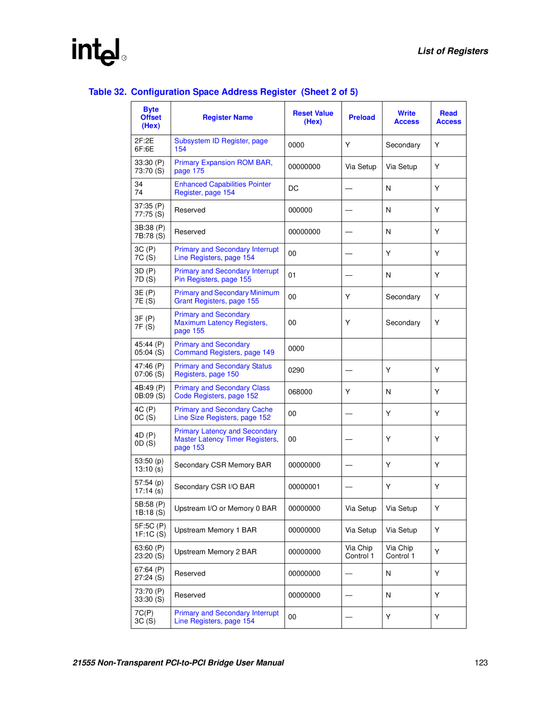
Configuration Space Address Register Sheet 2
Configuration Space Address Register Sheet 3
Configuration Space Address Register Sheet 4
CSR Address Map Sheet 1
Configuration Space Address Register Sheet 5
Register Name Reset Value Write Access Read Access
Control and Status Registers
CSR Address Map Sheet 2
CSR Address Map Sheet 3
Ffff W1TS
Ffff W1TC
CSR Address Map Sheet 4
Primary CSR and Downstream Memory 0 Bara Sheet 1
Address Decoding
Primary and Secondary Address
CSR Address Map Sheet 5
Secondary CSR Memory BARsa Sheet 1
Primary CSR and Downstream Memory 0 Bara Sheet 2
Secondary CSR Memory BARsa Sheet 2
Primary and Secondary CSR I/O Barsa
Offsets Primary CSR I/O BAR Secondary CSR I/O BAR
Downstream I/O or Memory 1 and Upstream I/O or Memory 0 BAR
Offsets
Upstream I/O or Memory 0 BAR
Downstream Memory 2 and 3 BAR, and Upstream Memory 1 BAR
Upstream Memory 2 Bar
Upper 32 Bits Downstream Memory 3 Bar
Offsets Downstream I/O or Memory
Translated Base
Xlatbase
Downstream Upstream Offsets Memory Translated Base
Upstream I/O or Memory Setup
139
Upper 32 Bits Downstream Memory 3 Setup Register
Configuration Transaction Generation Registers
Cfgaddr
Downstream and Upstream Configuration Address Registers
Cfgdata
Configuration Own Bits Register
Configuration CSR Sheet 1
Ioaddr IA
Configuration CSR Sheet 2
Downstream I/O Address and Upstream I/O Address Registers
Offset Downstream I/O Address Upstream I/O Address
Iodata
Downstream I/O Data and Upstream I/O Data Registers
O Own Bits Registers
Offsets Downstream I/O Data Upstream I/O Data
O CSR
Lookup Table Offset Register
Lutoffset
Upstream Memory 2 Lookup Table
Configuration Registers
PCI Registers
Lookup Table Data Register
Device ID Register
Primary Interface Configuration Space Address Map
Secondary Interface Configuration Space Address Map
Vendor ID Register
Primary and Secondary Command Registers
Primary and Secondary Command Registers Sheet 1
Offsets Primary Command Secondary Command
Offsets Primary Status Secondary Status
Primary and Secondary Command Registers Sheet 2
Primary and Secondary Status Registers Sheet 1
SERR#
Revision ID Rev ID Register
Primary and Secondary Status Registers Sheet 2
Offsets Primary Cache Line Size Secondary Cache Line Size
Primary and Secondary Class Code Registers
Primary and Secondary Cache Line Size Registers
Offsets Primary Class Code Secondary Class Code
Header Type Register
BiST Register
Offsets Primary MLT Secondary MLT
Primary and Secondary Interrupt Line Registers
Subsystem Vendor ID Register
Subsystem ID Register
Enhanced Capabilities Pointer Register
Primary and Secondary Interrupt Pin Registers
Primary and Secondary Minimum Grant Registers
Primary and Secondary Maximum Latency Registers
Device-Specific Control and Status Registers
Device-Specific Control and Status Address Map
Chip Control 0 Register Sheet 1
Chip Control 0 Register Sheet 2
Chip Control 0 Register Sheet 3
Chip Control 0 Register Sheet 4
Chip Control 1 Register Sheet 1
Chip Control 1 Register Sheet 2
Chip Control 1 Register Sheet 3
Chip Status Register
I20ENA
163
Rots
Generic Own Bits Register
I2O Inbound PostList Status
16.6 I2O Registers
I2O Outbound PostList Status
I2O Outbound PostList Interrupt Mask
I2OOUT P
I2O Inbound PostList Interrupt Mask
I2O Inbound Queue
I2O Outbound Queue
I2O Outbound PostList Head Pointer
I2O Inbound FreeList Head Pointer
I2O Inbound PostList Tail Pointer
I2O Outbound FreeList Tail Pointer
Ldifc W1TLS
I2O Inbound PostList Counter
I2O Inbound FreeList Counter
Ldipc W1TLS
I2O Outbound PostList Counter
I2O Outbound FreeList Counter
Ldopc W1TLS
PMD0 W1TC
Interrupt Registers
Chip Status CSR
Chip Set IRQ Mask Register
Chip Clear IRQ Mask Register
Upstream Page Boundary IRQ 0 Register
PAGE0IRQ W1TC
Upstream Page Boundary IRQ 1 Register
Upstream Page Boundary IRQ Mask 0 Register
Upstream Page Boundary IRQ Mask 1 Register
Primary Set IRQ
Primary Clear IRQ and Secondary Clear IRQ Registers
Primary Set IRQ and Secondary Set IRQ Registers
Primary Clear IRQ Secondary Clear IRQ
Secondary Set IRQ Mask
Primary Set IRQ Mask and Secondary Set IRQ Mask Registers
Scratchpad 0 Through Scratchpad 7 Registers Sheet 1
Primary Clear IRQ Mask Secondary Clear IRQ Mask
Prom Registers
Scratchpad 0 Through Scratchpad 7 Registers Sheet 2
Primary Expansion ROM BAR
Sequence on
Primary Expansion ROM Setup Register
ROM Setup Register
ROM Data Register
Romdata
ROM Address Register
ROM Control Register Sheet 1
Romaddr
Srompoll
Mode Setting Configuration Register Sheet 1
Srom Registers
ROM Control Register Sheet 2
Mode Setting Configuration Register Sheet 2
Serial Preload Sequence Sheet 1
Byte Description Offset
Serial Preload Sequence Sheet 2
Serial Preload Sequence Sheet 3
Arbiter Control
Error Registers
Secondary SERR# Disable Register
Primary SERR# Disable Register
Power Management ECP ID and Next Pointer Register
Init Registers
PM ECP ID
PME
Power Management Capabilities Register
APS
DSI
Pmcsr Bridge Support Extensions
Power Management Control and Status Register
Reset Control Register
Power Management Data Register
HS Next Pointer
CompactPCI Hot-Swap Control Register Sheet 1
Jtag Registers
CompactPCI Hot-Swap Control Register Sheet 2
Jtag Instruction Register Options Sheet 1
Boundary Scan Order
Jtag Instruction Register Options Sheet 2
Bypass Register
Boundary-Scan Register
VPD Registers
Vital Product Data VPD ECP ID and Next Pointer Register
VPD ECP
VPD Data Register
Vital Product Data VPD Address Register
Page
Acronyms
Acronyms
CSR
Index
140