Toshiba Corporation
File Number
Copyright
Satellite A10/TECRA A1/Satellite Pro A10 Maintenance Manual
Safety Precautions
Preface
Satellite A10/TECRA A1/Satellite Pro A10 Maintenance Manual
Conventions
Acronyms
Table of Contents
Chapter Tests and Diagnostics
Chapter Replacement Procedures
HDD
Appendices
Satellite A10/TECRA A1/Satellite Pro A10 Maintenance Manual
Hardware Overview
Hardware Overview
Chapter Contents
Figures
Tables
Difference of each model
Features
Features Hardware Overview
Model a Model B Model C Model D Model E Model F
Hardware Overview Features
LCD
LAN/MODEM
Front of the computer and the system units configuration
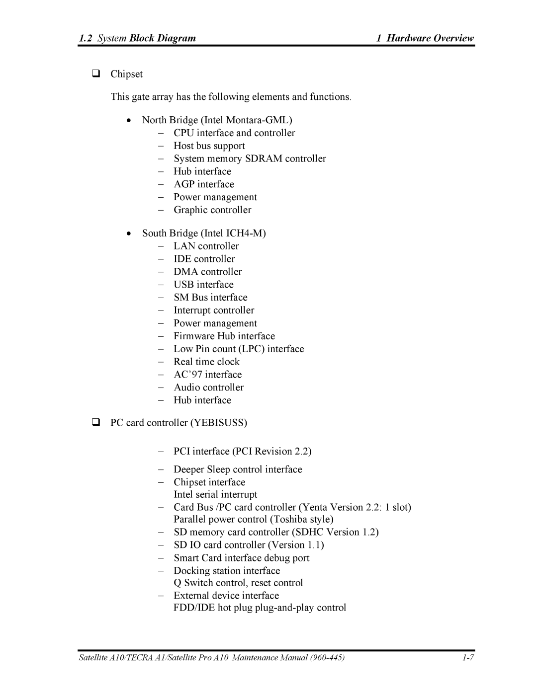
System Block Diagram
System Block Diagram Hardware Overview
Hardware Overview System Block Diagram
CPU
System Block Diagram Hardware Overview
Hardware Overview System Block Diagram
3.5-inchUSB Floppy Disk Drive Hardware Overview
3.5-inch USB Floppy Disk Drive
2DD 2HD
2.5-inch Hard Disk Drive
2.5-inch HDD dimensions 2/3
Hardware Overview 2.5-inchHard Disk Drive
2.5-inch HDD Specifications 1/3
2.5-inch HDD dimensions 3/3
2.5-inchHard Disk Drive Hardware Overview
Inch HDD Specifications 3/3
Inch HDD Specifications 2/3
Specifications
CD-ROMDrive Hardware Overview
CD-ROM Drive
Teac G8CC00005810
DVD-ROM Drive
Hardware Overview DVD-ROMDrive
Specifications Toshiba G8CC0000R810
DVD-ROM drive dimensions 1/2
DVD-ROM drive dimensions 2/2
Specifications Hitachi G8CC00015H10
Toshiba SDR2412OAA
Combo Drive
Hardware Overview Combo Drive
CD-DA, CD+EG, CD-MIDI, CD-TEXT, CD-ROM, CD
Combo Drive Hardware Overview
Combo drive specifications 2/5
Combo drive specifications 3/5
Teac G8CC0000Q810
Teac G8CC0001D810
Combo drive specifications 4/5
Combo drive specifications 5/5
Panasonic G8CC0001C810
Combo+2 drive
Specifications Toshiba G8CC0000ZH10
Combo+2 drive Hardware Overview
Hardware Overview DVD Multi drive
Specifications Panasonic G8CC00019810
DVD Multi drive
2MB DVD DVD-VIDEO, DVD-ROM CD-R, CD-RW
Keyboard
Keyboard Hardware Overview
Hardware Overview TFT Color Display
TFT Color Display
LCD Module
10 LCD module specifications 15.0-inch SXGA+ TFT 3/3
10 LCD module specifications 14.1-inch XGA TFT 1/3
10 LCD module specifications 15.0-inch XGA TFT 2/3
Specifications G33C0000P110 G33C0000N110 G33C0000R110
FL Inverter Board
11 FL inverter board specifications
DC5
Power Supply
Power Supply Hardware Overview
Hardware Overview Power Supply
12 Power supply output rating
Battery Name Output Capacity Element
Battery specifications
Main Battery
Batteries
Hardware Overview Batteries
Battery Charging Control
14 Time required for charges of main battery
15 Data preservation time
16 Time required for charges of RTC battery
RTC Battery
Condition Time
Hardware Overview AC Adapter
17 AC adapter specifications
AC Adapter
G71C00002T G71C00002S
Chapter Troubleshooting Procedures
Troubleshooting Procedures
Power Status Check
Troubleshooting Procedures
Battery icon
Troubleshooting Procedures
Troubleshooting
Troubleshooting Troubleshooting Procedures
Troubleshooting Flowchart
Troubleshooting Procedures Troubleshooting Flowchart
Troubleshooting Flowchart Troubleshooting Procedures
Troubleshooting flowchart 1/2
Troubleshooting flowchart 2/2
Troubleshooting Flowchart Troubleshooting Procedures
Procedure 1 Power Status Check
Power Supply Troubleshooting
Troubleshooting Procedures Power Supply Troubleshooting
Battery icon
DC in icon Power supply status
Power Supply Troubleshooting Troubleshooting Procedures
DC in icon
Procedure 2 Error Code Check
Error code Meaning
Second Battery
1R5-C1V output P62
E5V output
1R25-B1V output
Power Supply Troubleshooting Troubleshooting Procedures
Procedure 3 Connection Check
Procedure 4 Charging Check
Procedure 5 Replacement Check
System Board Troubleshooting
Troubleshooting Procedures System Board Troubleshooting
System Board Troubleshooting Troubleshooting Procedures
Procedure 1 Message Check
KBC Error HDC Error
Procedure 2 Printer Port LED Check on Boot Mode
Printer port LED
LED
Printer port LED boot mode status 1/8
LED Status Test item Contents
FDC Reset
Printer port LED boot mode status 2/8
UPDATE/DAMAGED, Bios UPDATE/DAMAGED
Beep
Printer port LED boot mode status 3/8
Printer port LED boot mode status 4/8
Printer port LED boot mode status 5/8
ROM
Printer port LED boot mode status 6/8
Printer port LED boot mode status 7/8
Printer port LED boot mode status 8/8
LED Status Test item Contents
System Board Troubleshooting Troubleshooting Procedures
Procedure 3 Printer Port LED Check on Suspend/Resume Mode
Printer port LED suspend mode error status 1/3
Printer port LED suspend mode error status 2/3
ROM
Printer port LED suspend mode error status 3/3
Printer port LED resume mode error status 1/4
Printer port LED resume mode error status 2/4
Printer port LED resume mode error status 3/4
Printer port LED resume mode error status 4/4
Procedure 4 Diagnostic Test Program Execution Check
3.5 FDD Troubleshooting Troubleshooting Procedures
3.5 FDD Troubleshooting
Procedure 1 FDD Head Cleaning Check
FDD error code and status
Troubleshooting Procedures 3.5 FDD Troubleshooting
Procedure 2 Diagnostic Test Program Execution Check
Code Status
Procedure 3 Connector Check and Replacement Check
PJ4600
Troubleshooting Procedures 2.5 HDD Troubleshooting
2.5 HDD Troubleshooting
Procedure 1 Partition Check
2.5 HDD Troubleshooting Troubleshooting Procedures
Procedure 2 Message Check
Procedure 3 Format Check
2.5 Hard disk drive error code and status
Procedure 5 Connector Check and Replacement Check
Procedure 1 Diagnostic Test Program Execution Check
Keyboard Troubleshooting
Keyboard Troubleshooting Troubleshooting Procedures
Procedure 2 Connector Check and Replacement Check
Procedure 2 Connector and Cable Check
Display Troubleshooting
Troubleshooting Procedures Display Troubleshooting
PJ5600
Display Troubleshooting Troubleshooting Procedures
Procedure 3 Replacement Check
Touch Pad Troubleshooting
Troubleshooting Procedures Touch Pad Troubleshooting
Optical Drive Troubleshooting
Optical Drive Troubleshooting Troubleshooting Procedures
Modem Troubleshooting
Troubleshooting Procedures Modem Troubleshooting
LAN Troubleshooting
LAN Troubleshooting Troubleshooting Procedures
Troubleshooting Procedures Sound Troubleshooting
Sound Troubleshooting
Procedure 2 Connector Check
Sound Troubleshooting Troubleshooting Procedures
Troubleshooting Procedures Wireless LAN Troubleshooting
Wireless LAN Troubleshooting
Procedure 1 Transmitting-Receiving Check
Procedure 2 Antennas Connection Check
Wireless LAN Troubleshooting Troubleshooting Procedures
Mini PCI
Procedure Antenna Check
Procedure 4 Replacement Check
Troubleshooting Procedures Wireless LAN Troubleshooting
Chapter Tests and Diagnostics
Tests and Diagnostics
Chapter Contents
27.1 Function Description Accessing the Setup Program
Diagnostic Test
Diagnostic Test Tests and Diagnostics
Tests and Diagnostics Diagnostic Test
Executing the Diagnostic Test
Executing the Diagnostic Test Tests and Diagnostics
Tests and Diagnostics Executing the Diagnostic Test
System Test Name
Tests and Diagnostics3.2 Executing the Diagnostic Test
Subtest names 1/2
Subtest Names Tests and Diagnostics
Subtest Names
Test Name Subtest No Subtest Name
Tests and Diagnostics Subtest Names
Subtest names 2/2
System Test Tests and Diagnostics
System Test
Tests and Diagnostics System Test
EXT. Temp =
Tests and Diagnostics Memory Test
Memory Test
Memory Test Tests and Diagnostics
Tests and Diagnostics Keyboard Test
Keyboard Test
Keyboard Test Tests and Diagnostics
Pointing Parameter
Test port number select 1Port2, 2Port3, 0Port2&3 ?
Tests and Diagnostics Display Test
Display Test
Display Test Tests and Diagnostics
Display example Mode
Tests and Diagnostics Display Test
Floppy Disk Test Tests and Diagnostics
Floppy Disk Test
Tests and Diagnostics Floppy Disk Test
Printer Test Tests and Diagnostics
Printer Test
Tests and Diagnostics Printer Test
Async Test Tests and Diagnostics
Async Test
Tests and Diagnostics Async Test
Async Test Tests and Diagnostics
Tests and Diagnostics Hard Disk Test
Hard Disk Test
Hard Disk Test Tests and Diagnostics
Worst pattern data Cylinder
‘B5ADAD’
Real Timer Test
Real Timer Test Tests and Diagnostics
Tests and Diagnostics Real Timer Test
NDP Test Tests and Diagnostics
NDP Test
Sub# Address Good Bad Contents
Tests and Diagnostics Expansion Test
Expansion Test
Expansion Test Tests and Diagnostics
Tests and Diagnostics CD-ROM/DVD-ROM Test
CD-ROM/DVD-ROM Test
LAN Test Tests and Diagnostics
LAN Test
Tests and Diagnostics Sound/LAN/Modem Test
Sound/LAN/Modem Test
Sound/LAN/Modem Test Tests and Diagnostics
Press any key, and the following message appear
When the subtest is executed, the following message appears
After a few seconds, the following message will appear
Wireless LAN Test Agere
Tests and Diagnostics Wireless LAN Test Agere
Wireless LAN Test Agere Tests and Diagnostics
Transmit test
Receive test
Wireless LAN Test Agere3 Tests and Diagnostics
This Card is WEP Press any key to continue
Wireless LAN Test Atheros
Wireless LAN Test Atheros Tests and Diagnostics
Setting the responder machine
Tests and Diagnostics Wireless LAN Test Atheros
Setting the tester machine
Then the test returns to the main menu automatically
Diagnostics
Error Code and Error Status Names
Error Code and Error Status Names
Error codes and error status names 1/3
Error codes and error status names 2/3
Diagnostics Error Code and Error Status Names
ZVCONT\ Error
Error codes and error status names 3/3
Card Type Error
No Pcmcia
Hard disk controller status register contents
Diagnostics Hard Disk Test Detail Status
Hard Disk Test Detail Status
Error register contents
Function Description
FDD Cleaning
Diagnostics FDD Cleaning
Operations
Log Utilities Diagnostics
Log Utilities
Diagnostics Log Utilities
Running Test Diagnostics
Running Test
Mount the work disks on the drives, then press Enter key
Floppy Disk Drive Utilities
Floppy Disk Drive Utilities
Diagnostics Floppy Disk Drive Utilities
Following message will appear
Select a format type and the following message will appear
Following message will appear. To finish the dump, select
System Configuration
Diagnostics System Configuration
Press Enter to return to the Diagnostic Menu
Setup
Diagnostics Setup
Setup Diagnostics
Accessing the Setup Program
Configuration
Factory Preset Configuration
Moving Within the Setup Menu and Changing Values
Accepting Changes and Exiting the Setup Window
Password Write Policy
Setup Options
System Date Sets the date System Time Sets the time
User Setting
Details, see Battery Save Options below
Bright Full brightness for high visibility
Setup Diagnostics
PXE
Boot Turns on boot mode. Default Resume Turns on resume mode
Enabled
All Devices
LPT setting Interrupt level Address
Pcic Compatible
ECP
PCI LAN
Chapter Replacement Procedures
Replacement Procedures
MDC Modem
18.7 Replacing Inch XGA Samsung Fluorescent Lamp
Removing Battery Cover
45 to Replacing 14.1 Inch TMD fluorescent lamp 1 to 65 to
Vii
Viii
Overview Replacement Procedures
Overview
Replacement Procedures Overview
Safety Precautions
Before You Begin
Disassembly Procedures
Assembly Procedure
Tools and Equipment
Screw Tightening Torque
Grip Color
Screw Notation
Replacement Procedures Battery Pack/PC Card
Battery Pack/PC Card
Battery Pack Removing the battery pack
Battery Pack/PC Card Replacement Procedures
Removing Battery Pack
Installing the battery pack
Installing the PC card
PC Card Removing the PC card
Memory Module
Replacement Procedures Memory Module
Removing the memory module
Memory Module Replacement Procedures
Installing the memory module
HDD
Replacement Procedures HDD
Removing the HDD
HDD Replacement Procedures
Removing HDD Assy
Removing HDD
Installing the HDD
MDC Modem
Replacement Procedures MDC Modem
Removing the MDC Modem
MDC Modem Replacement Procedures
Installing the MDC Modem
Mini PCI Card
Replacement Procedures Mini PCI Card
Removing the Mini PCI Card
Mini PCI Card Replacement Procedures
Installing the Mini PCI Card
Fan Module/Cooling Fin/CPU
Replacement Procedures Fan Module/Cooling Fin/CPU
Removing the Fan Module/Cooling Fin/CPU
Fan Module/Cooling Fin/CPU Replacement Procedures
13 Removing Fan Module
14 Removing CPU Holder
15 Removing Cooling Fin
Installing the Fan Module/Cooling Fin/CPU
17 Installing the CPU
18 Applying Silicon Grease
Replacement Procedures Keyboard
Removing the keyboard
Keyboard Replacement Procedures
20 Removing Keyboard Hold Plate
21 Removing Keyboard Support Plate
Installing the keyboard
Optical Drive
Replacement Procedures Optical Drive
Removing the Optical Drive
Optical Drive Replacement Procedures
23 Removing CD-ROM Drive
Installing the Optical Drive
Display Assembly Replacement Procedures
Display Assembly
Removing the Display Assembly
Replacement Procedures Display Assembly
25 Removing Display Assembly
26 Removing Display Assembly
Installing the Display Assembly
Touch Pad
Touch Pad Replacement Procedures
Removing the Touch Pad
Replacement Procedures Touch Pad
Installing the Touch Pad
BAT CON Holder
BAT CON Holder Replacement Procedures
Installing the BAT CON Holder
Removing the BAT CON Holder
Replacement Procedures System Board/DC-IN Jack/RTC Battery
System Board/DC-IN Jack/RTC Battery
Removing the System Board/DC-IN Jack/RTC Battery
System Board/DC-IN Jack/RTC Battery Replacement Procedures
29 Removing System Board
30 Removing FIR Dummy Cover
Installing the System Board/DC-IN Jack/RTC Battery
Removing the BAT Lock ASSY/HDD Upper Assy
31 Removing BAT Lock Assy
32 Removing HDD Upper Assy
Installing the BAT Lock ASSY/HDD Upper Assy
Removing the Touch Pad Switch
Touch Pad Switch
Touch Pad Switch Replacement Procedures
Installing the Touch Pad Switch
LCD Unit/FL Inverter
Replacement Procedures LCD Unit/FL Inverter
Removing the LCD Unit/FL Inverter
LCD Unit/FL Inverter Replacement Procedures
35 Removing FL Inverter and LCD Unit
36 Removing LCD Bracket
Installing the FL Inverter/LCD Unit
Wireless LAN Antenna/Display Cover/Speaker
Removing the Wireless LAN Antenna/Display Cover/Speaker
38 Removing Speaker Cables
39 Removing Wireless LAN Antennas
40 Removing Hinge Cover
41 Removing Speakers
42 Removing LCD Cable Holder
43 Removing Display Cover
44 Removing Hinges
Installing the Wireless LAN Antenna/Display Cover/Speaker
Satellite A10/TECRA A1/Satellite Pro A10 Maintenance Manual
Fluorescent Lamp
Replacement Procedures Fluorescent Lamp
Type Supplier Section
Replacing the TMD 14.1 Inch XGA Fluorescent Lamp
Fluorescent Lamp Replacement Procedures
Disassembling Fluorescent Lamp
46 Replacing 14 Inch TMD fluorescent lamp
47 Replacing 14 Inch TMD fluorescent lamp
48 Replacing 14 Inch TMD fluorescent lamp
49 Replacing 14 Inch TMD fluorescent lamp
Assembling Fluorescent Lamp
50 Replacing 14 Inch TMD fluorescent lamp
51 Replacing 14 Inch TMD fluorescent lamp
Be careful not to damage the TAB
52 Replacing 14 Inch TMD fluorescent lamp
53 Replacing 14 Inch TMD fluorescent lamp
54 Replacing 14 Inch TMD fluorescent lamp
55 Replacing 14 Inch TMD fluorescent lamp
56 Replacing 14 Inch TMD fluorescent lamp
Replacing the 14.1 Inch XGA Chimei Fluorescent Lamp
58 Replacing 14.1 Inch Chimei fluorescent lamp
59 Replacing 14.1 Inch Chimei fluorescent lamp
62 Replacing 14.1 Inch Chimei fluorescent lamp
Remove the screw
64 Replacing 14.1 Inch Samsung fluorescent lamp VF2058P01
65 Replacing 14.1 Inch Samsung fluorescent lamp VF2058P01
66 Replacing 14.1 Inch Samsung fluorescent lamp VF2058P01
68 Replacing 14.1 Inch Samsung fluorescent lamp VF2058P01
70 Replacing 14.1 Inch Samsung fluorescent lamp VF2058P01
71 Replacing 14.1 Inch Samsung fluorescent lamp VF2058P01
72 Replacing 14.1 Inch Samsung fluorescent lamp VF2048P01
75 Replacing 14.1 Inch Samsung fluorescent lamp VF2048P01
76 Replacing 14.1 Inch Samsung fluorescent lamp VF2048P01
78 Replacing 14.1 Inch Samsung fluorescent lamp VF2048P01
79 Replacing 14.1 Inch Samsung fluorescent lamp VF2048P01
81 Replacing 14.1 Inch Samsung fluorescent lamp VF2048P01
Replacing the 14.1 Inch XGA LG.Philips Fluorescent Lamp
82 Replacing 14.1 Inch LG.Philips fluorescent lamp
83 Replacing 14.1 Inch LG.Philips fluorescent lamp
84 Replacing 14.1 Inch LG.Philips fluorescent lamp
85 Replacing 14.1 Inch LG.Philips fluorescent lamp
86 Replacing 14.1 Inch LG.Philips fluorescent lamp
87 Replacing 14.1 Inch LG.Philips fluorescent lamp
88 Replacing 14.1 Inch LG.Philips fluorescent lamp
89 Replacing 14.1 Inch LG.Philips fluorescent lamp
Replacement Procedures Fluorescent Lamp
90 Replacing 15.0 Inch LG.Philips fluorescent lamp XGA
92 Replacing 15.0 Inch LG.Philips fluorescent lamp XGA
93 Replacing 15.0 Inch LG.Philips fluorescent lamp XGA
Assembling the 15.0-inch XGA LG.Philips Fluorescent Lamp
96 Replacing 15.0 Inch LG.Philips fluorescent lamp XGA
97 Replacing 15.0 Inch LG.Philips fluorescent lamp XGA
98 Replacing 15.0 Inch Samsung fluorescent lamp XGA
99 Replacing 15.0 Inch Samsung fluorescent lamp XGA
102 Replacing 15.0 Inch Samsung fluorescent lamp XGA
103 Replacing 15.0 Inch Samsung fluorescent lamp XGA
105 Replacing 15.0 Inch Samsung fluorescent lamp XGA
Assembling the 15.0-inch XGA Samsumg Fluorescent Lamp
107 Replacing 15.0 Inch Sharp fluorescent lamp XGA
108 Replacing 15.0 Inch Sharp fluorescent lamp XGA
110 Replacing 15.0 Inch Sharp fluorescent lamp XGA
112 Replacing 15.0 Inch Sharp fluorescent lamp XGA
113 Replacing 15.0 Inch Sharp fluorescent lamp XGA
114 Replacing 15.0 Inch Sharp fluorescent lamp XGA
116 Replacing 15.0 Inch Sharp fluorescent lamp XGA
Assembling the 15.0 Inch XGA Sharp Fluorescent Lamp
118 Replacing 15.0 Inch Sharp fluorescent lamp XGA
120 Replacing 15.0 Inch Sharp fluorescent lamp XGA
122 Replacing 15.0 Inch Sharp fluorescent lamp XGA
124 Replacing 15.0 Inch Sharp fluorescent lamp XGA
126 Replacing 15.0 Inch Sharp fluorescent lamp XGA
128 Replacing 15.0 Inch Sharp fluorescent lamp XGA
129 Replacing 15.0 Inch Sharp fluorescent lamp XGA
130 Replacing 15.0 Inch Chimei fluorescent lamp XGA
131 Replacing 15.0 Inch Chimei fluorescent lamp XGA
132 Replacing 15.0 Inch Chimei fluorescent lamp XGA
134 Replacing 15.0 Inch Chimei fluorescent lamp XGA
Assembling the 15.0 Inch XGA Chimei fluorescent lamp
136 Replacing 15.0 Inch LG.Philips fluorescent lamp SXGA+
137 Replacing 15.0 Inch LG.Philips fluorescent lamp SXGA+
139 Replacing 15.0 Inch LG.Philips fluorescent lamp SXGA+
Assembling the 15.0 Inch SXGA+ LG.Philips Fluorescent Lamp
141 Replacing 15.0 Inch LG.Philips fluorescent lamp SXGA+
143 Replacing 15.0 Inch LG.Philips fluorescent lamp SXGA+
144 Replacing 15.0 Inch Samsung fluorescent lamp SXGA+
145 Replacing 15.0 Inch Samsung fluorescent lamp SXGA+
147 Replacing 15.0 Inch Samsung fluorescent lamp SXGA+
149 Replacing 15.0 Inch Samsung fluorescent lamp SXGA+
151 Replacing 15.0 Inch Samsung fluorescent lamp SXGA+
Assembling the 15.0 Inch SXGA+Samsung Fluorescent Lamp
Discard the tapes removed. Do not reuse them
153 Replacing 15.0 Inch Sharp fluorescent lamp SXGA+
154 Replacing 15.0 Inch Sharp fluorescent lamp SXGA+
156 Replacing 15.0 Inch Sharp fluorescent lamp SXGA+
158 Replacing 15.0 Inch Sharp fluorescent lamp SXGA+
160 Replacing 15.0 Inch Sharp fluorescent lamp SXGA+
162 Replacing 15.0 Inch Sharp fluorescent lamp SXGA+
Assembling the 15.0 Inch SXGA+ Sharp Fluorescent Lamp
164 Replacing 15.0 Inch Sharp fluorescent lamp SXGA+
166 Replacing 15.0 Inch Sharp fluorescent lamp SXGA+
167 Replacing 15.0 Inch Sharp fluorescent lamp SXGA+
169 Replacing 15.0 Inch Sharp fluorescent lamp SXGA+
170 Replacing 15.0 Inch Sharp fluorescent lamp SXGA+
172 Replacing 15.0 Inch Sharp fluorescent lamp SXGA+
174 Replacing 15.0 Inch Sharp fluorescent lamp SXGA+
176 Replacing 15.0 Inch Sharp fluorescent lamp SXGA+
177 Replacing 15.0 Inch Sharp fluorescent lamp SXGA+
Appendices
Appendices
Appendix Contents
Appendix D
Figure B-1
Table C-21
Precautions for handling the LCD module
Apx. a Handling the LCD Module Appendices
Appendices Apx. a Handling the LCD Module
Apx. a Handling the LCD Module Appendices
Appendices Apx. a Handling the LCD Module
Apx. a Handling the LCD Module Appendices
Appendices Apx. a Handling the LCD Module
System Board Front View
Apx. B Board Layout Appendices
Appendices Apx. B Board Layout
Table B-1 System board ICs and connectors front
Mark Number Name
System Board Back View
Figure B-2 System board layout back
Table B-2 System board ICs and connectors back
Pin No Signal name Signal Name
System Board PJ1420 Memory 0 Connector 200-pin
Table C-1 Memory 0 connector pin assignment 200-pin 1/4
Apx. C Pin Assignment Appendices
Table C-1 Memory 0 connector pin assignment 200-pin 2/4
Appendices Apx. C Pin Assignment
Table C-1 Memory 0 connector pin assignment 200-pin 3/4
Table C-1 Memory 0 connector pin assignment 200-pin 4/4
SCK3-B2P
PJ1440 Memory 1 Connector 200-pin
Table C-2 Memory 1 connector pin assignment 200-pin 1/4
SCK3-B2N GND SDQ20R-B2P SDQ21R-B2P SDQ17R-B2P SDQ16R-B2P
Table C-2 Memory 1 connector pin assignment 200-pin 2/4
Table C-2 Memory 1 connector pin assignment 200-pin 3/4
Table C-2 Memory 1 connector pin assignment 200-pin 4/4
CDAUDL-PXP CDAUDR-PXP CD-GND IDRSTB-P5N
PJ1800 Optical Drive I/F Connector 50-pin
Table C-3 Optical drive I/F connector pin assignment 50-pin
SDDREQ-P5P GND SDIOR-P3N SDIOW-P3N SIORDY-P5P SDDACK-P3N
IDRSTA-P5N GND
PJ1801 HDD I/F Connector 44-pin
Table C-4 HDD I/F connector pin assignment 44-pin
GND PDDREQ-P3P PDIOW-P3N PDIOR-P3N PIORDY-P3P PDDACK-P3N
PJ2001 PC Card I/F Connector 68-pin
Table C-5 PC card I/F connector pin assignment 68-pin 1/2
Table C-5 PC Card slot connector pin assignment 68-pin2/2
PJ2200 Mini PCI I/F Connector 124-pin
Table C-6 Mini PCI I/F connector pin assignment 124-pin 1/2
Table C-5 Mini PCI I/F connector pin assignment 124-pin 2/2
CBE0-P3N
Table C-7 MDC I/F connector pin assignment 30-pin
PJ3000 MDC I/F Connector 30-pin
PJ3203 Debug Port Connector 4-pin
Table C-8 Debug port connector pin assignment 4-pin
Table C-9 Keyboard connector pin assignment 34-pin
PJ3333 Keyboard Connector 34-pin
10 PJ3201 Touch Pad I/F Connector 4-pin
Table C-10 Touch pad I/F connector pin assignment 4-pin
Table C-11 Parallel I/F connector pin assignment 25-pin
11 PJ3202 Parallel I/F Connector 25-pin
12 PJ4100 Network I/F Connector 12-pin
Table C-12 Network I/F connector pin assignment 12-pin
Table C-13 USB I/F connector pin assignment 8-pin
13 PJ4600 USB I/F Connector 8-pin
14 PJ5600 LCD I/F Connector 40-pin
Table C-14 LCD I/F connector pin assignment 40-pin
17 PJ6002 External Microphone Connector 6-pin
15 PJ5620 CRT I/F Connector 15-pin
16 PJ5640 TV Connector 4-pin
Apx. C Pin AssignmentAppendices
20 PJ6004 Headphone Connector 6-pin
18 PJ6000 Speaker Connector Left 3-pin
19 PJ6001 Speaker Connector Right 2-pin
21 PJ8810 1st Battery Connector 10-pin
23 PJ8770 FAN I/F Connector 3-pin
22 PJ8790 RTC Battery Connector 3-pin
24 PJ8800 DC-IN Connector 4-pin
Appendices Apx. C Pin Assignment
Apx. D Keyboard Scan/Character Codes Appendices
Display Codes
Table D-1 Display Codes
Appendices Apx. D Keyboard Scan/Character Codes
Keyboard Layout
Apx. E Key LayoutAppendices
Appendices Apx. E Key Layout
Apx. E Key Layout Appendices
Appendices Apx. E Key Layout
Parallel Port Wraparound Connector
Apx. F Wiring Diagrams Appendices
RGB Monitor ID Wraparound Connector 15-Pin to 15-Pin
Appendices Apx. F Wiring Diagrams
Appendix G BIOS/KBC/EC Update
Apx. G BIOS/KBC/EC Update Appendices
Appendices Apx. G BIOS/KBC/EC Update
Apx. H Reliability Appendices
Table H-1 Mtbf
Appendices Apx. H Reliability