UG081 v6.0 June 1
MicroBlaze Processor Reference Guide
MicroBlaze Processor Reference Guide
Date Version Revision
MicroBlaze Processor Reference Guide UG081 v6.0 June 1
UG081 v6.0 June 1
Preface About This Guide
MicroBlaze Application Binary Interface
Additional Resources
Manual Contents
Typographical
Conventions
Conventions Meaning or Use Example
Online Document
UG081 v6.0 June 1
Overview
Features
Version Status Deprecated Active
MicroBlaze Architecture
Instructions
Data Types and Endianness
FSR
MSR
ESR
EAR
Op1 if cond else op2
MicroBlaze Processor Reference Guide
MicroBlaze Processor Reference Guide UG081 v6.0 June 1
MicroBlaze Processor Reference Guide
MicroBlaze Processor Reference Guide UG081 v6.0 June 1
Registers
Registers
General Purpose Registers
Special Purpose Registers
Program Counter PC
PVR
8Program Counter PC Bits Name Description Reset Value
Machine Status Register MSR
9Machine Status Register MSR Bits Name Description
FSL
EIP
DCE
ICE
Exception Address Register EAR
Buslock Enable
ESS
Exception Status Register ESR
Source/Destination Register
Branch Target Register BTR
Processor Version Register PVR
Floating Point Status Register FSR
Cusediv
CFG
Cusebarrel
DIV
Cunalignedexception
Cdebugenabled
OP0EXEC
Unexec
Ccachebytesize
Icll
Cicachelinelen
Icbs
Rstmsr
Cresetmsr
Pipeline Architecture
Arch
Delay Slots
Memory Architecture
Branches
Reset, Interrupts, Exceptions, and Break
Reset, Interrupts, Exceptions, and Break
Exception Causes
Reset
Hardware Exceptions
Equivalent Pseudocode
Hardware Breaks
Breaks
Latency
Interrupt
User Vector Exception
Software Breaks
Instruction Cache
Instruction Cache
Overview
General Instruction Cache Functionality
MSR Bit
Data Cache
Instruction Cache Operation
Instruction Cache Software Support
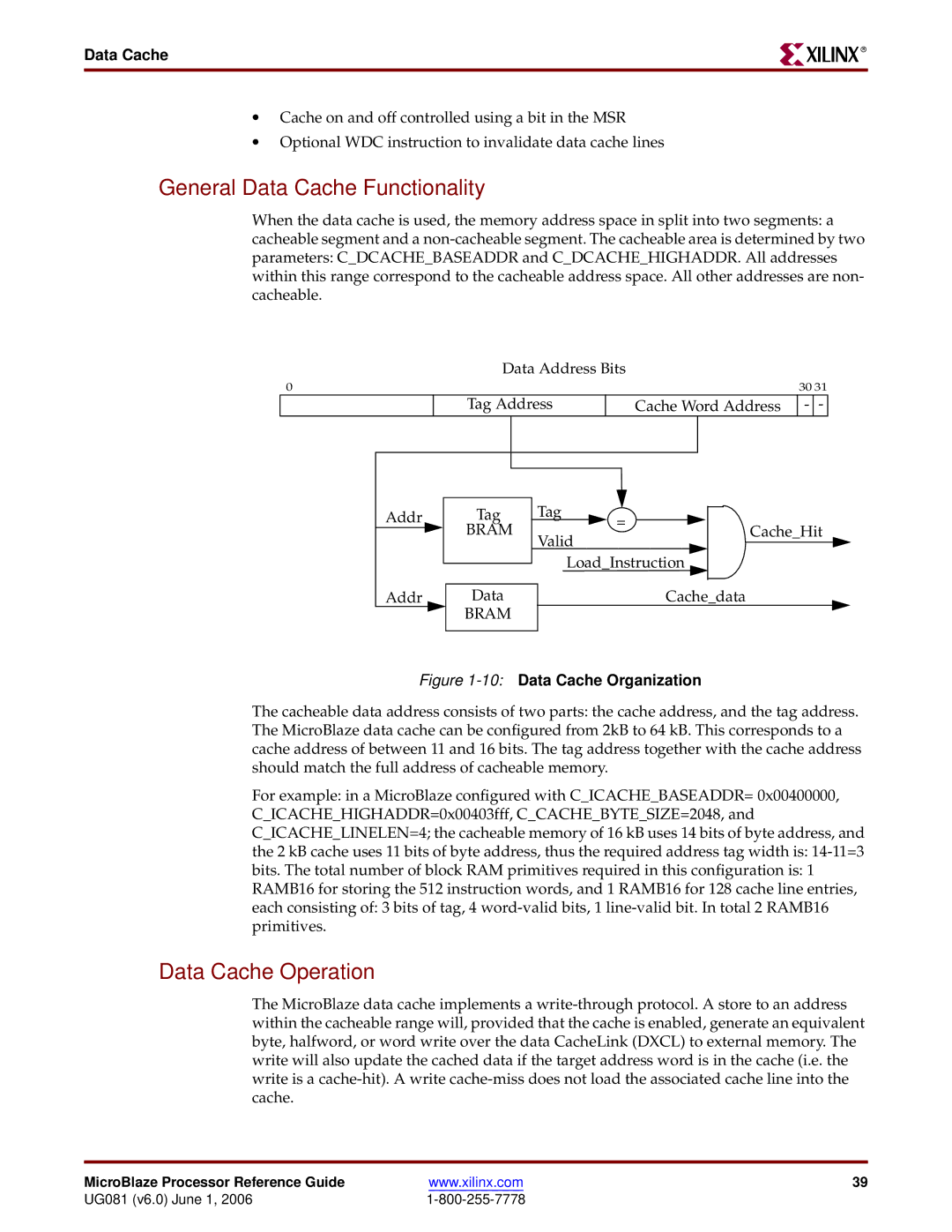
General Data Cache Functionality
Data Cache Operation
Data Cache
Floating Point Unit FPU
Data Cache Software Support
WDC Instruction
Arithmetic
Format
Rounding
Operations
Comparison
Hardware Acceleration using FSL
Fast Simplex Link FSL
Exceptions
Debug and Trace
Debug Overview
Trace Overview
MicroBlaze Architecture
Dxcl
MicroBlaze I/O Overview
Ilmb
Ixcl
Dmrnw Dopb
MicroBlaze Signal Interface Description
Mfsl
Imrnw Iopb
DAS Dlmb
IAS Ilmb
Dxclm
On-Chip Peripheral Bus OPB Interface Description
Ixclm
Dxcls
Addr031
LMB Signal Interface
ByteEnable03
Local Memory Bus LMB Interface Description
DataRead031
DataWrite031
ReadStrobe
WriteStrobe
LMB Transactions
Generic Write Operation
Generic Read Operation
BE0 BE1 BE2
Back-to-Back Write Operation
Single Cycle Back-to-Back Read Operation
Back-to-Back Mixed Read/Write Operation
Read and Write Data Steering
RD1623 RD2431
RD07 RD815 RD1623 RD2431
Master FSL Signal Interface
Slave FSL Signal Interface
Fast Simplex Link FSL Interface Description
FSL BUS Read Operation
Xilinx CacheLink XCL Interface Description
FSL Transactions
FSL BUS Write Operation
CacheLink Signal Interface
CacheLink Transactions
Instruction Cache Read Miss
Data Cache Read Miss
Data Cache Write
MDM
Debug Interface Description
Trace Interface Description
Debug Interface Description
MicroBlaze Processor Reference Guide
11 Type of Trace Exception TraceExceptionKind Description
MicroBlaze Core Configurability
Values Assigned Type
Cnumberofrdaddrbrk
Cusepcmpinstr
Cusemsrinstr
Pcmpne Cunalignedexception
Ffff
Cicacheusefsl
Cdcacheusefsl
Data Types
Scope
Register Usage Conventions
MicroBlaze Application Binary Interface
2Register usage conventions Type Enforcement Purpose
Stack Convention
Stack Convention
High Memory Low Memory Func
Memory Model
Interrupt and Exception Handling
1Symbol notation Meaning
Summary
Notation
Opcode Destination Reg Source Reg a Immediate Value
Formats
Type a
Type B
Add
Description
Registers Altered
Addi
RD, rA, rB
Registers Altered Latency
Logial and with Immediate Andi RD, rA, IMM
Andi
Andn
Logical and not
Andn RD, rA, rB
Logical and not with Immediate Andni RD, rA, IMM
Andni
Beq
Branch if Equal Beq
Beqd
Beqi
Branch Immediate if Equal Beqi
Beqid
Bge
Branch if Greater or Equal Bge
Bged
Bgei
Branch Immediate if Greater or Equal Bgei
Bgeid
Bgt
Branch if Greater Than Bgt
Bgtd
Bgti
Branch Immediate if Greater Than Bgti
Bgtid
Ble
Branch if Less or Equal Ble
Bled
Blei
Branch Immediate if Less or Equal Blei
Bleid
Branch if Less Than Blt
Blt
Blti
Blti
Bltid
Bne
Branch if Not Equal Bne
Bned
Bnei
Branch Immediate if Not Equal Bnei
Bneid
Brad
Instructions Unconditional Branch
Bra
Brd
MicroBlaze Instruction Set Architecture
Bri
MicroBlaze Instruction Set Architecture
Msrbip
Instructions BrkBreak RD, rB
Break Immediate Brki RD, IMM
Brki
Instructions Barrel Shift Bsrl
Bsra
Bsll
Bslli
Bsi
Barrel Shift Immediate Bsrli
Bsrai
Cmp
Integer Compare Cmp
Cmpu
Fadd
Floating Point Arithmetic Add Fadd
Esrec FSRIO,UF,OF,DO
Frsub
Reverse Floating Point Arithmetic Subtraction
Frsub RD, rA, rB Reverse subtract
Floating Point Arithmetic Multiplication Fmul
Fmul
Esrec FSRIO,UF,OF,DO,DZ
Fdiv
Floating Point Arithmetic Division
Fdiv RD, rA, rB Divide
Fcmp
Esrec FSRIO,DO
Cget
Get
Get from fsl interface
Nget
Idiv
Integer Divide Idiv
Idivu
Immediate ImmIMM
Imm
Lbu
Load Byte Unsigned
Lbu RD, rA, rB
Load Byte Unsigned Immediate Lbui RD, rA, IMM
Lbui
Lhu RD, rA, rB
Lhu
Load Halfword Unsigned Immediate Lhui RD, rA, IMM
Lhui
Load Word
Load Word Immediate Lwi RD, rA, IMM
Lwi
Mfs RD, rS
Mfs
Read MSR and clear bits in MSR Msrclr RD, Imm
Msrclr
Msrset RD, Imm
Msrset
Move To Special Purpose Register Mts RS, rA
Mts
Instructions Mul Multiply RD, rA, rB
Multiply Immediate Muli RD, rA, IMM
Muli
Logical or
Logical or with Immediate Ori RD, rA, IMM
Ori
Pattern Compare Byte Find Pcmpbf
Pcmpbf
Pattern Compare Equal Pcmpeq
Pcmpeq
Pattern Compare Not Equal Pcmpne
Pcmpne
Cput
Put
Put to fsl interface
Nput
Rsubk
Rsub
Arithmetic Reverse Subtract Rsub
Rsubc
Rsubik
Rsubi
Arithmetic Reverse Subtract Immediate Rsubi
Rsubic
Rtbd
Return from Break
Rtbd RA, IMM
Rtid
Return from Interrupt Rtid RA, IMM
Msrie
Rted
Return from Exception Rted RA, IMM
Msree Msreip ESR
Return from Subroutine Rtsd RA, IMM
Rtsd
None
Store Byte Immediate Sbi RD, rA, IMM
Sbi
Sext16 RD, rA
Sext16
Sext8
Sign Extend Byte
Sext8 RD, rA
Instructions Store Halfword RD, rA, rB
Store Halfword Immediate Shi RD, rA, IMM
Shi
Sra RD, rA
Sra
Shift Right with Carry Src RD, rA
Src
Srl
Shift Right Logical
Srl RD, rA
Addr ← rA + rB Addr3031 ← MemAddr ← rD031
Store Word Immediate Swi RD, rA, IMM
Register Altered
Write to Data Cache
Wdc
Wic
Logical Exclusive or Xor RD, rA, rB
Xor
Xori
Logical Exclusive or with Immediate
Xori RA, rD, IMM
148