Page
Inter
Intel Corporation
Table of Contents
Chapter Architectural Compatibility
Chapter Highlights
Page
High-performance Implementation
32-bit Architecture
Highlights
Configurable Protection
Virtual Memory Support
Extended Debugging Support
Summary
Object Code Compatibility
Application Architecture
Page
Registers
General Registers
Flags and Instruction Pointer
Numeric Coprocessor Registers
Memory and logical Addressing
Logical Address Translation
Segment and Descriptor Registers
Addressing Modes
Principal Data Types
Data Types and Instructions
Numeric Coprocessor Data Types
Other Instructions
Stack Instructions
~.,...I-------.-1 Byte String
LII
Miscellaneous Instructions
Chapter System Architecture
Page
Multitasking
System Registers
Task State Segment
Task Switching
Address Translation Overview
Addressing
Address Translation Overview
Segments
Principal Descriptor Fields
~~~~~.II~~~
Pages
Linear to Physical Address Translation
Virtual Memory
I I I
Privilege
Protection
USing Privilege Levels
Segment Protection
Privileged Instructions
Protection
10. Gates as Protected Entry Points
Interrupts and Exceptions
Interrupt Descriptor Table
Debug Eceptions and Registers
System Architecture
Page
Architectural Compatibility
Page
Real and Virtual 86 Modes
80286 Compatibility
Architectural Compatibility
Trapping Virtual 861\11ode System Calls
Page
Chapter Hardware Implementation
Page
Chapter Hardware Implementation
Hardware Implementation
Data and Address Buses
Clock
Bus Cycle Control
Bus Cycle Definition
Non-pipelined Bus Cycle Timing
Bus Cycles with Pipelined Addresses
Dynamic Bus Sizing
Processor Status and Control
Coprocessor Control
Mixed 16- and 32-bit Accesses
Chapter Data Sheet
Page
80386
Update Notice
Table of Contents
Privilege Validation
Descriptor Tables Introduction
Interrupt Descriptor Table
Segment Descriptor Cache
Functional Data
Pipelined Address with Dynamic Data Bus Sizing
Package Thermal Specification
3.4
Initiating and Maintaining Pipelined Address
Register Overview
Base Architecture Introduction
Flags Register
Register Descriptions
General Purpose Registers
Instruction Pointer
TSS
Segment Registers
Segment Registers Descriptor Registers Loaded Automatically
Other Segment Physical Base Address Segment Limit
MSW
Segment Descriptor Registers
Control Registers
Flects the current state of the ET bit
Directory Base Register CR3
TS Task Switched, bit
Fault Linear Address Register CR2
System Address Registers
Register Accessibility
Debug and Test Registers
Compatibility
Idtr
Instruction Set Overview
Iopl
Gdtr
2b Arithmetic Instructions
2 80386 Instructions
2dLogical Instructions
2a Data Transfer
2h Protection Model
2e Bit Manipulation Instructions
2f. Program Control Instructions
2g High Level Language Instructions
Addressing Modes Overview
Register and Immediate Modes
3 32-Bit Memory Addressing Modes
Differences Between 16 and 32 Bit Addresses
Addressing Mode Calculations
None
Displacement
Data Types
Base Register BX,BP Index Register SI,DI Scale Factor
Sign ED rrrrrrrrl
LilliililillIl
Memory Organization
Introduction
Address Spaces
Segment Register Usage
I/O Space
Maskable Interrupt
Interrupts
Interrupts and Ecep~ions
Interrupt Processing
Software Interrupts
Non-Maskable Interrupt
NMI 2.INTR
Interrupt and Exception Priorities
Reset and Initialization
Double Fault
Instruction Restart
Debugging Support
TLB Testing
Testability
Self-Test
Breakpoint Instruction
Single-Step Trap
Debug Registers
DR4
DR1
DR2
DR3
Usage
Encoding Causing Breakpoint
Debug Status Register DR6
Real Mode Architecture Real Mode Introduction
ADD, OR, ADC, SBB
SET/RESET/COMPLEMENT
Memory Addressing
Xchg
Reserved Locations
Intierrupts
Shutdown and Halt
Addressing Mechanism
Protected Mode Addressing
Descriptor Tables Introduction
Segmentation Introduction
Terminology
Descriptor Tables
Segment Base 15 Segment Limit 15
Descriptors
Byte
Address
Dptm typ , data gm,nt
System Descriptor Formats
Offset 31
Selector
Offset 15
Word
Segment Descriptor Cache
Differences Between 386 and 286 Descriptors
Segment Base 15
Selector Fields
Nil R~L
~~~~~~~EL~~E~ ~A~~ ~I~I! ttl
~!~~~~E L~~E~~~s~ I~I! ~ J
~~?~~~~EL~~E~B~~E ~I~I~ tJ1
Protection Concepts
Rules of Privilege
Privilege Levels
Privilege Level Transfers
CALL, JMP
GOT/LOT
Call
RET,IRET
80386
Call Ga~es
Task Switching
Infef
Initialization and Transition to Protected Mode
Paging Concepts
Tools for Building Protected
Paging
Systems
Directory
Paging Organization
Mechanism
Descriptor Base Register
DIRECTORY/TABLE Entries
Level Protection R/W, U/S Bits
Frame Address 31 Reserved
Tables
Paging Operation
Translation Lookaside Buffer
Executing 8086 Programs
Paging In Virtual Mode
Access Type
Virtual 8086 Environment
24. Virtual 8086 Environment Memory Management
Protection and 1/0 Permission Bitmap
Entering and Leaving Virtual
Interrupt Handling
Task Switches TO/FROM Virtual 8086 Mode
For state saving i.e. push all registers in prolog, pop
·25.Virtual 8086 Environment Interrupt and Call Handling
Clock CLK2
Introduction
Address Bus BEO# through BE3#, A2 through A31
Data Bus do through
Bus Cycle Definition Signals W/R#, D/C#, MIIO#, LOCK#
Introduction
Bus Control Signals
Coprocessor Interface Signals
Bus Arbitration Signals
Interrupt Signals
Signal Summary
BEO#
Memory and 1/0 Spaces
Dynamic Data Bus Sizing
Memory and 110 Organization
Cycles 1 and 1a
Interfacing with 32- and 16-Bit Memories
BEO# BHE# BLE# AD
Operand Alignment
Li,\~~
P1 1.p2 .p1 1.p2 .p1 1.p2 .p1 1.p2 .p1 1.p2 .p1 1.p2 .p1
·9.Fastest Read Cycles with Pipelined Address Timing
Address Pipelining
Address signal A2 selects bank Bit datapath to each bank
TWO-BANK Interleaved Memory
FOUR-BANK Interleaved Memory
Introduction
Read and Write Cycles
Ixxx
NON-PIPELINED Address
Xxxxx Ixxxx
Xxxi Xxxix
13 80386 Bus States not usIng pipelined address
·14Asserting BS16# zero wait states, non·pipelinedaddress
3.3 NON·PIPELINED Address with Dynamic Data BUS Sizing
BSI6# XXX XXx XXX X .. IXXXXwOO~ J, XXX XXX1/ \
Xixxxxx Valid
Xixxxx ,XXXXY
~~~~ DOO¥
B516# ~~..tJ.~~~~~~~
Bus Sizing with Pipelined Address
BS16 # 44~~~...l-.lI...l Ready # 44~~.lI...l/l
~ ,T1-T~-T2PJ ,T1PT2PJ Idle non-pipelined pipelined
Pipelined
Acknowledge
IO#, D/c#
20 Complete Bus States including pipelined address
Ffi
~ -XXIXXY
Xxxxy ~j XDONTCAR~X~ x~ ~X~~lKX~ /..XXXX
Xxxxx IXXXXIXXXXI.. /..DXXXIXXX ~ Xxxxiy
Xxixxy ~ /..XIXXY
~--cp--- ----- ----- ----- ----- ~
Interrupt Acknowledge Inta Cycles
23.Halt Indication Cycle
Halt Indication Cycle
24. Shutdown Indication Cycle
Shutdown Indication Cycle
Entering and Exiting Hold Acknowledge
Reset During Hold Acknowledge
Bus Activity During and Following Reset
Other Functional Descriptions
26. Requesting Hold from Active Bus NA # negated
Component and Revision Identifiers
SELF-TEST Signature
Component Revision Stepping Identifier Name
Component Revision
CMD1
Software Testing for Coprocessor Presence
PIN Assignment
Mechanical Data Introduction
000 0 0 0 000 0 0
Vee Vss
1654189~1
Package Dimensions and Mounting
Measure PGA Case Temperature
Package Thermal Specification
Ill
Infef80386
Electrical Data
Power and Grounding
Maximum Ratings
D.C. Specifications
A.C. Specifications
1 A.C. Spec Definitions
102
2 A.C. Specification Tables
·4 -16 A.C. Characteristics Symbol Parameter 80386-16
Unit Min Max Operating Frequency MHz Half of CLK2
16 A.C. Characteristics Symbol Parameter
Symbol Parameter Min
80386-16 Min Unit Max
80386 ~QW~OOg OOOIP@OOIMl~iiO@OO
3 A.C. Test Loads 4 A.C. Timing Waveforms
106
MAX
Itm
PI~
80386 Instruction Encoding
Instruction SET
111
8o386Instructlon Set CIock Count Summary
112
·1 Instruction Set Clock Count Summary
RIm
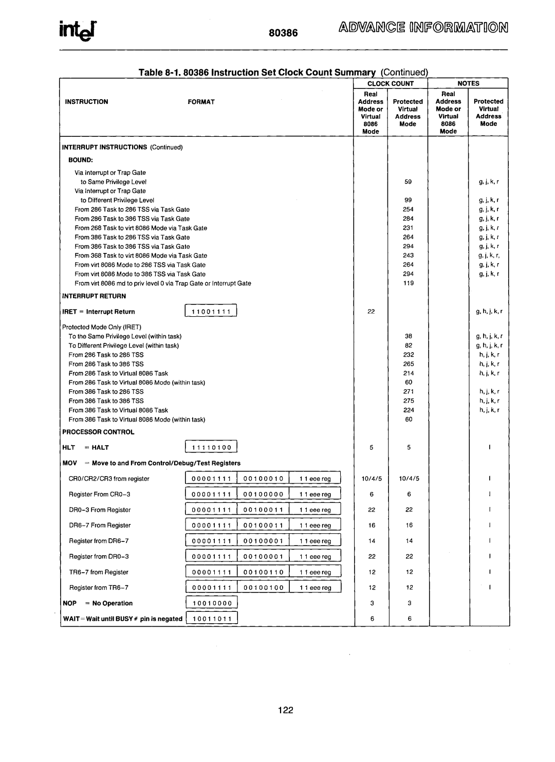
80386 Instructlon Set CIockCount S ummary Contlnued
Doubleword
·1 80386 Instruction Set Clock Count Summary
115
Instruction Set Clock Count Summary
BIT Manipulation
Instruction Set Clock Count Summarycontlnued
+ml 7+ml
Instruction Set Clock Count Summar
Protected
80386 Ins ruefIon SetCIoek CountSummary ConrInued
119
120
Interrupt Instructions
80386 Instructlon Set CIockCountSummaay Contmued
Bound
O3861nstructlon Set CIockCount Summary Contlnued
80386 nstructlon Set CIockCount Summary Contlnued
Infef80386
Madear
Ns ruetIon StCIe oekCount 5 ummary Contlnued
~~~\
Overview
Bits
2 32-Bit Extensions of the Instruction Set
Encoding of Instruction Fields
Field
Encoding of Address Mode
EOI
Osbx
OSBX+d16
11010
OS EAX
Scale Factor
NE/NZ
Encoding of Operation Direction
NAE
NB/AE
California
Domestic Sales Offices
United States