Data Manual
Data Manual
FIXED-POINT Digital Signal Processor
C64x+ Peripheral Information and Electrical Specifications
Recommended Operating Conditions
FIXED-POINT Digital Signal Processor
Enhanced Turbo Decoder Coprocessor TCP2
Features
ZTZ/GTZ BGA Package Bottom View
Description
ZTZ/GTZ 697-PIN Ball Grid Array BGA Package Bottom View
Submit Documentation Feedback
Functional Block Diagram
Functional Block Diagram
Hardware Features
Device Characteristics
Characteristics of the C6455 Processor
C6455
CPU DSP Core Description
FIXED-POINT Digital Signal Processor
C64x+ CPU DSP Core Data Paths
Memory Map Summary
C6455 Memory Map Summary
Memory Block Description Block Size Bytes HEX Address Range
03FF Ffff
02CF Ffff
02DF Ffff
0FFF Ffff
Boot Sequence
Boot Modes Supported
FIXED-POINT Digital Signal Processor
2 2nd-Level Bootloaders
Pin Assignments
Pin Map
C6455 Pin Map Bottom View Quadrant B
C6455 Pin Map Bottom View Quadrant C
C6455 Pin Map Bottom View Quadrant D
Signal Groups Description
Gpio
TINPL1 TOUTL1
TINPL0
URADDR4/PCBE0/GP2C SYSCLK4/GP1A
ACE2A
ACE5A ACE4A
ACE3A
ABE7 ABE6 ABE5 ABE4
CLKR1/GP0
HCNTL0/PSTOP HCNTL1/PDEVSEL HHWIL/PCLK HPI16 only
Hpia
Clks Shared
UXADDR4/MDCLK
UXADDR3/MDIO
Rgmdio
URSOC/MRXER/RMRXER
UXDATA1/MTXD1/RMTXD1
UXDATA4/MTXD4
URDATA3/MRXD3 UXDATA3/MTXD3 URDATA2/MRXD2 UXDATA2/MTXD2
UXDATA0/MTXD0/RMTXD0
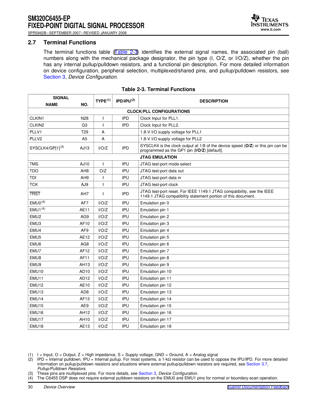
Terminal Functions
Signal
IPD/IPU Description Name CLOCK/PLL Configurations
Terminal Functions
Signal Name
Type 1 IPD/IPU
Emifa 64 BIT Control Signals Common to ALL Types of Memory
Emifa 64 BIT BUS Arbitration
Emifa 64 BIT ASYNCHRONOUS/SYNCHRONOUS Memory Control
AEA1916
Signal TYPE1 Name
IPD/IPU2 Description Emifa 64 BIT Address
AEA15
AEA5
IPD/IPU Description Name
AEA6
AEA4
Signal TYPE1 IPD/IPU2 Description Name Emifa 64 BIT Data
AED19
AED21
AED20
AED18
IPD/IPU2 Description
DDR2 Memory Controller 32 BIT Address
Timer
IPD/IPU Description Name DDR2 Memory Controller 32 BIT Data
INTER-INTEGRATED Circuit I2C
Multichannel Buffered Serial Port 0 McBSP0
Signal TYPE1 IPD/IPU2 Description Name
Multichannel Buffered Serial Port 1 McBSP1
Utopia Slave ATM Controller Transmit Interface
URADDR2/PINTA1/ GP14 URADDR1/PRST
TYPE1 IPD/IPU2 Description
Utopia Slave ATM Controller Receive Interface
Signal TYPE1 IPD/IPU2 Description Name Rapidio Serial Port
Management Data INPUT/OUTPUT Mdio for MII/RMII/GMII
Management Data INPUT/OUTPUT Mdio for Rgmii
Device Configuration
RSV07 RSV09
Rgrefclk
RSV05
Reserved for Test
RSV15
RSV13
RSV14
RSV16
Signal TYPE1 Name no
IPD/IPU2 Description Supply Voltage Monitor Pins
Supply Voltage Pins
U16
AA1 AA6
AB7
AC6 AC9
AF1
AD5 AD7
AE6 AE8
CV DD
Ground Pins
Cvdd
GND
F20 F22 F24 G11 G13 G15 G17 G19 G21 G23
M16 M18 M24 M26 M29 N13 N15 N17 N19 N23 P12 P14 P16 P18
AA2 AA7
AB6
AC7 AC8
GND AF2
AD6
AE4 AE7
AH1
Device Support
Development
Development Support
Device and Development-Support Tool Nomenclature
SM=Qualifieddevice
C6000 DSP platforms
FIXED-POINT Digital Signal Processor
Configuration IPD PIN
Device Configuration at Device Reset
C6455 Device Configuration Pins AEA190, ABA10, and Pcien
IPU1
AEA12
AEA14
AEA13
AEA11
IPU
Peripheral Configuration at Device Reset
Configuration IPD Functional Description PIN
ABA0
Lower Upper
Configuration PIN Setting Utopiaen Pcien PIN
UTOPIAEN, and MACSEL10 Peripheral Selection Utopia and Emac
AUTO-INIT
State
Peripheral Selection After Device Reset
Peripheral States
Peripherals That can be This State
Static Powerdown Reset Enable Progress Disabled Enabled
Unlock the PERCFG0 register by Using the Perlock register
Device State Control Registers
Device State Control Registers
HEX Address Range Acronym Register Name
Bit Field Value Description 310
Peripheral Lock Register Description
Lockval
Lockval
Peripheral Configuration Register 0 Description
Bit Field Value Description
Bit Field
Peripheral Configuration Register 1 Description
DDR2CTL Emifactl
DDR2CTL
Peripheral Status Registers Description
Hpistat
I2CSTAT
1715
SM320C6455-EP
Utopiastat Pcistat
Utopiastat
Emac Configuration Register Emaccfg Description
Rmiirst
Emulator Buffer Powerdown Register Emubufpd Description
Emuctl
Sysclkout MCBSP1EN PCI66
Device Status Register Description
Emifaen DDR2EN Pcien CFGGP2 CFGGP1 CFGGP0
Pcieeai MACSEL1 MACSEL0
Pcieeai
MACSEL10
Utopiaen
Variant Part Number Manufacturer LSB
BOOTMODE30
Jtag ID Jtagid Register Description
Variant
Configuration Examples
Pullup/Pulldown Resistors
HPI VCP2 HRDY,HINT
FIXED-POINT Digital Signal Processor
Internal Buses, Bridges, and Switch Fabrics
System Interconnect
Data Switch Fabric Connections
Switched Central Resource Block Diagram
Configuration Switch Fabric
SCR Connection Matrix
C64x+ Megamodule SCR Connection
C6455 Default Bus Master Priorities
BUS Master Default Priority Control Priority Level
Bus Priorities
X+ Megamodule Block Diagram
Memory Architecture
C6455 L1P Memory Configurations
C6455 L2 Memory Configurations
Available Memory Page Protection Schemes
Memory Protection
Bandwidth Management
AID0 Bit
Megamodule Reset Global or Local
Power-Down Control
Megamodule Resets
Reset Type Megamodule
Version
Megamodule Revision
Version Revision a
Revision
C64x+ Megamodule Register Descriptions
Megamodule Interrupt Registers
Megamodule Powerdown Control Registers
Megamodule Revision Register
Megamodule Idma Registers
Megamodule Cache Configuration Registers
MAR168 Controls Emifa CE2 Range A800 0000 A8FF Ffff
Megamodule L1/L2 Memory Protection Registers
L2MPPA6
L2MPPA4
L2MPPA5
L2MPPA7
L1PMPPA20
L1PMPPA18
L1PMPPA19
L1PMPPA21
11. Device Configuration Registers Chip-Level Registers
10. CPU Megamodule Bandwidth Management Registers
HEX Address Range Acronym Register Name Comments
MIN NOM MAX Unit
Recommended Operating Conditions
DV DD12, DV DDRM, AV DDT, AV DDA
AV DDA
Recommended Operating Conditions
VSS VIH VIL
VOS
TDO DVDD33 = MIN IOH = MAX
Parameter Test CONDITIONS1 MIN TYP MAX Unit
VOH VOL
DVDD33 = MIN IOL = MAX
Current DC
1 3.3-V Signal Transition Levels
2 3.3-V Signal Transition Rates
Parameter Information
Timing Parameters and Board Routing Analysis
Power-Supply Sequencing
Recommended Clock and Control Signal Transition Behavior
Power Supplies
Power-Supply Decoupling
108
Enhanced Direct Memory Access EDMA3 Controller
C6455 EDMA3 Channel Synchronization Events1
EDMA3 Device-Specific Information
EDMA3 Channel Synchronization Events
Edma Binary Event Name Event Description Channel
EDMA3 Peripheral Register Descriptions
C6455 EDMA3 Channel Synchronization Events
EDMA3 Channel Controller Registers
DCHMAP10
DCHMAP8
DCHMAP9
DCHMAP11
DCHMAP57
DCHMAP55
DCHMAP56
DCHMAP58
DRAE6
DRAE5
DRAEH5
DRAEH6
QSTAT2
QSTAT0
QSTAT1
QSTAT3
Shadow Region 0 Channel Registers
Interrupt Enable Register High
EDMA3 Parameter RAM1
EDMA3 Transfer Controller 0 Registers
EDMA3 Transfer Controller 1 Registers
EDMA3 Transfer Controller 2 Registers
121
EDMA3 Transfer Controller 3 Registers
123
10. C6455 System Event Mapping
Interrupts
Interrupt Sources and Interrupt Controller
Event Number Interrupt Event Description
XINT1
XINT0
RINT1
TINTLO0
L1PCMPA
L1PED1
Pdcint
L1PDMPA
External Interrupts Electrical Data/Timing
11. Timing Requirements for External Interrupts1 see Figure
NMI
12. Reset Types
Reset Controller
Power-on Reset POR Pin
Type Initiator
Warm Reset Reset Pin
Max Reset
System Reset
CPU Reset
Reset Priority
Srst Mrst Wrst POR
Reset Controller Register
Reset Type Status Register Description
Srst
720 1000/-1000 Unit
Reset Electrical Data/Timing
14. Timing Requirements for Reset12 3see -8and Figure
Parameter
Power-Up Timing
Resetstat
CLKIN1 CLKIN2 POR
PLL1 and PLL1 Controller
1 PLL1 Controller Device-Specific Information
Internal Clocks and Maximum Operating Frequencies
16. PLL1 Clock Frequency Ranges
1.3 PLL1 Stabilization, Lock, and Reset Times
Clock Signal MIN MAX Unit
1.2 PLL1 Controller Operating Modes
2 PLL1 Controller Memory Map
17. PLL1 Stabilization, Lock, and Reset Times
18. PLL1 Controller Registers Including Reset Controller
MIN TYP
Pllrst
3 PLL1 Controller Register Descriptions
3.1 PLL1 Control Register
Pllpwrdn
PLL Multiplier Control Register
20. PLL Multiplier Control Register Pllm Field Descriptions
PLL Pre-Divider Control Register
Preden
Ratio
PLL Controller Divider 4 Register
D4EN
PLL Controller Divider 5 Register
D5EN
PLL Controller Command Register
Goset
PLL Controller Status Register
Gostat
PLL Controller Clock Align Control Register
Plldiv Ratio Change Status Register
SYS5 SYS4
SYS5
Sysclk Status Register
SYS5ON SYS4ON SYS3ON SYS2ON
29. Timing Requirements for CLKIN1 Devices123 see Figure
PLL Modes
SYSCLK4
23. PLL2 Block Diagram
PLL2 and PLL2 Controller
1.2 PLL2 Controller Operating Modes
1 PLL2 Controller Device-Specific Information
31. PLL2 Clock Frequency Ranges
Pllref Pllen =
32. PLL2 Controller Registers
2 PLL2 Controller Memory Map
3 PLL2 Controller Register Descriptions
HEX Address Range Acronym Description
PLL Controller Divider 1 Register
D1EN
155
ALN1
SYS1
SYS1ON
4 PLL2 Controller Input Clock Electrical Data/Timing
39. Timing Requirements for CLKIN2123 see Figure
DDR2 Memory Controller
1 DDR2 Memory Controller Device-Specific Information
2 DDR2 Memory Controller Peripheral Register Descriptions
3 DDR2 Memory Controller Electrical Data/Timing
40. DDR2 Memory Controller Registers
External Memory Interface a Emifa
Emifa Device-Specific Information
Emifa Peripheral Register Descriptions
41. Emifa Registers
Emifa Electrical Data/Timing
42. Timing Requirements for Aeclkin for EMIFA12 see Figure
Aeclkin
See -33and Figure
Aeclkin AECLKOUT1
ABA10 AED630 Read Data
Setup = Hold =
ACEx ABE70
AAOE/ASOE a AAWE/ASWE a AR/W Aardy B Deasserted
Strobe Setup = Extended Strobe
ABA10 AED630
Aeclkout Aardya Asserted Deasserted
Setup time, read AEDx valid before Aeclkout high
EA1 EA2 EA3 EA4
SM320C6455-EP
BE1 BE2 BE3 BE4
ASADS/ASRE B AAOE/ASOE B AAWE/ASWEB
Write Latency =
DSP Owns Bus
HOLD/HOLDA Timing
HHOLDAL-HOLDL Hold time, Hold low after Holda low
Hold Holda
Delay time, Aeclkout high to Abusreq valid AECLKOUTx
Busreq Timing
11 I2C Peripheral
11.1 I2C Device-Specific Information
I2CXSR
I2COAR
I2CCLKH I2CSAR
I2CEMDR
11.2 I2C Peripheral Register Descriptions
51. I2C Registers
Standard Mode Fast Mode MIN MAX
11.3 I2C Electrical Data/Timing
SDA SCL
Stop Start
Start Stop
43. I2C Transmit Timings
Stop Start Repeated
HPI Peripheral Register Descriptions
Host-Port Interface HPI Peripheral
HPI Device-Specific Information
54. HPI Control Registers
HPI Electrical Data/Timing
See -56through Figure
NO.PARAMETER
HR/W Hhwil Hstrobea
HCS Has
HCNTL10
HD150
HR/W Hhwil Hstrobe a
Hrdyb
46. HPI16 Write Timing has Not Used, Tied High
47. HPI16 Write Timing has Used
48. HPI32 Read Timing has Not Used, Tied High
49. HPI32 Read Timing has Used
Has input HCNTL10 Input HR/W input
Input HCS input
51. HPI32 Write Timing has Used
Input HCS input HD310 input
Multichannel Buffered Serial Port McBSP
McBSP Device-Specific Information
58. McBSP 1 Registers
McBSP Electrical Data/Timing
720 850 1000/-1000
FIXED-POINT Digital Signal Processor
Clks Clkr
Clkx
Clks
Clkx FSX
Master Slave MIN MAX
MASTER3 Slave MIN MAX
Bit Bitn-1
Setup time, DR valid before Clkx high 18P
Master Slave MIN
Hold time, DR valid after Clkx high + 36P
198
199
Ethernet MAC Emac
Ethernet Bus
Emac Device-Specific Information
Interface Modes
70. EMAC/MDIO Multiplexed Pins MII, RMII, and Gmii Modes
Ball Number Device PIN Name
Rmii
Interface Mode Clocking
Emac Peripheral Register Descriptions
71. Ethernet MAC Emac Control Registers
RX6FREEBUFFER
Macconfig
Softreset
RX7FREEBUFFER
72. Emac Statistics Registers
HEX Address Range Acronym
73. Emac Control Module Registers
74. Emac Descriptor Memory
02C8 2000 02C8 3FFF Emac Descriptor Memory
Mrclk Input
Emac Electrical Data/Timing
Mbps Gmii Only
Mtclk
Mrclk Input MRXD7−MRXD4GMII only
Gmtclk
Output
MRXD3−MRXD0
Mtxen Outputs
Mtclk Input MTXD7−MTXD4GMII only
MTXD3−MTXD0
Gmtclk Output
Emac Rmii Electrical Data/Timing
Rmrefclk Input
MRXD1-MRXD0 Mcrsdv
Mrxer Inputs 720 1000/-1000 Unit
Emac Rgmii Electrical Data/Timing
Cycle time, TXC Mbps 40*t cTXC 60*t cTXC
70. Emac Transmit Interface Timing Rgmii OperationAB
Management Data Input/Output Mdio
Mdio Device-Specific Information
Mdio Peripheral Register Descriptions 89. Mdio Registers
Mdio input
Delay time, Mdclk low to Mdio data output valid 100
Mdclk
Mdio output
Timers Peripheral Register Descriptions
Timers
Timers Device-Specific Information
92. Timer 0 Registers
Timers Electrical Data/Timing
94. Timing Requirements for Timer Inputs1 see Figure
TINPLx TOUTLx
16.2 VCP2 Peripheral Register Descriptions
Enhanced Viterbi-Decoder Coprocessor VCP2
16.1 VCP2 Device-Specific Information
96. VCP2 Registers
Tbhd
Enhanced Turbo Decoder Coprocessor TCP2
17.1 TCP2 Device-Specific Information
Tbsd
17.2 TCP2 Peripheral Register Descriptions
97. TCP2 Registers
Peripheral Component Interconnect PCI
98. Default Values for PCI Configuration Registers
Register Default Value
PCI Device-Specific Information
99. PCI Configuration Registers
PCI Peripheral Register Descriptions
100. PCI Back End Configuration Registers
101. DSP-toPCI Address Translation Registers
102. PCI Hook Configuration Registers
103. PCI External Memory Space
HEX Address Offset Acronym Register Name
4A7F Ffff
48FF Ffff
49FF Ffff
4AFF Ffff
PCI Electrical Data/Timing
104. Utopia Registers
Utopia Device-Specific Information
Utopia Peripheral Register Descriptions
105. Utopia Data Queues Receive and Transmit Registers
Uxclk
Utopia Electrical Data/Timing
106. Timing Requirements for UXCLK1 see Figure
Urclk
Uxclk UXDATA70
UXADDR40
Uxclav Uxenb Uxsoc
Urclk URDATA70 URADDR40 N Urclav Urenb Ursoc
P48 0x1F
Serial RapidIO Peripheral Register Descriptions
Serial RapidIO Srio Port
Serial RapidIO Device-Specific Information
112. RapidIO Control Registers
RIOBLK3EN
RIOBLK2EN
RIOBLK2ENSTAT
RIOBLK3ENSTAT
RIODOORBELL3ICSR
RIODOORBELL2ICSR
RIODOORBELL2ICCR
RIODOORBELL3ICCR
RIOERRRSTEVNTICRR3
Rioerrrstevnticrr
RIOERRRSTEVNTICRR2
RIOINTDST0DECODE
RIOLSU4REG2
RIOLSU4REG0
RIOLSU4REG1
RIOLSU4REG3
RIOQUEUE6RXDMAHDP
RIOQUEUE4RXDMAHDP
RIOQUEUE5RXDMAHDP
RIOQUEUE7RXDMAHDP
RIORXUMAPL1
RIORXUMAPL0
RIORXUMAPH0
RIORXUMAPH1
RapidIO Peripheral-Specific Registers
Riobaseid
Riolclcfghbar
Riolclcfgbar
Riohostbaseidlock
RIOSP0ERRDET
Rioctrlcapt
Riopwtgtid
RIOSP0RATEEN
Serial RapidIO Electrical Data/Timing
245
Gpio Peripheral Register Descriptions
General-Purpose Input/Output Gpio
Gpio Device-Specific Information
113. Gpio Registers
Pulse duration, GPOx high 36P 8
Gpio Electrical Data/Timing
114. Timing Requirements for Gpio Inputs12 see Figure
Pulse duration, GPOx low 36P 8
Emulation Features and Capability
Advanced Event Triggering AET
Trace
Jtag Device-Specific Information
Delay time, TCK low to TDO valid
Ieee 1149.1 Jtag
116. Timing Requirements for Jtag Test Port see Figure
See ADDITIONS/MODIFICATIONS/DELETIONS
Revision History
C6455 Revision History
Added 0.83 ns C6455-1200 1.2-GHz CPU Cycle Time
Packaging Information
Thermal Resistance Characteristics S-PBGA Package ZTZ/GTZ
Thermal Data
AIR Flow
Orderable Device Status Package Pins Package Eco Plan
MSL Peak Temp
Qty
Page
Products Applications
DSP
Rfid