www.ti.com
EMAC Functional Architecture
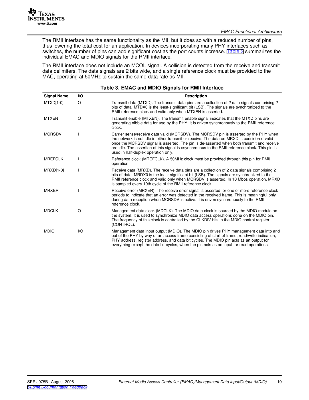
The RMII interface has the same functionality as the MII, but it does so with a reduced number of pins, thus lowering the total cost for an application. In devices incorporating many PHY interfaces such as switches, the number of pins can add significant cost as the port counts increase. Table 3 summarizes the individual EMAC and MDIO signals for the RMII interface.
The RMII interface does not include an MCOL signal. A collision is detected from the receive and transmit data delimiters. The data signals are 2 bits wide, and a single reference clock must be provided to the MAC, operating at 50MHz to sustain the same data rate as MII.
|
| Table 3. EMAC and MDIO Signals for RMII Interface |
Signal Name | I/O | Description |
O | Transmit data (MTXD). The transmit data pins are a collection of 2 data signals comprising 2 | |
|
| bits of data. MTDX0 is the |
|
| RMII reference clock and valid only when MTXEN is asserted. |
MTXEN | O | Transmit enable (MTXEN). The transmit enable signal indicates that the MTXD pins are |
|
| generating nibble data for use by the PHY. It is driven synchronously to the RMII reference |
|
| clock. |
MCRSDV | I | Carrier sense/receive data valid (MCRSDV). The MCRSDV pin is asserted by the PHY when |
|
| the network is not idle in either transmit or receive. The data on MRXD is considered valid |
|
| once the MCRSDV signal is asserted. The pin is |
|
| are idle. The assertion of this signal is asynchronous to the RMII reference clock. This pin is |
|
| used in |
MREFCLK | I | Reference clock (MREFCLK). A 50MHz clock must be provided through this pin for RMII |
|
| operation. |
I | Receive data (MRXD). The receive data pins are a collection of 2 data signals comprising 2 | |
|
| bits of data. MRDX0 is the |
|
| RMII reference clock and valid only when MCRSDV is asserted. In 10 Mbps operation, MRXD |
|
| is sampled every 10th cycle of the RMII reference clock. |
MRXER | I | Receive error (MRXER). The receive error signal is asserted for one or more reference clock |
|
| periods to indicate that an error was detected in the received frame. This is meaningful only |
|
| during data reception when MCRSDV is active. It is driven synchronously to the RMII |
|
| reference clock. |
MDCLK | O | Management data clock (MDCLK). The MDIO data clock is sourced by the MDIO module on |
|
| the system. It is used to synchronize MDIO data access operations done on the MDIO pin. |
|
| The frequency of this clock is controlled by the CLKDIV bits in the MDIO control register |
|
| (CONTROL). |
MDIO | I/O | Management data input output (MDIO). The MDIO pin drives PHY management data into and |
|
| out of the PHY by way of an access frame consisting of start of frame, read/write indication, |
|
| PHY address, register address, and data bit cycles. The MDIO pin acts as an output for |
|
| everything except the data bit cycles, when the pin acts as an input for read operations. |
SPRU975B | Ethernet Media Access Controller (EMAC)/Management Data Input/Output (MDIO) | 19 |
Submit Documentation Feedback |
|
|