www.ti.com
|
| EMAC Functional Architecture |
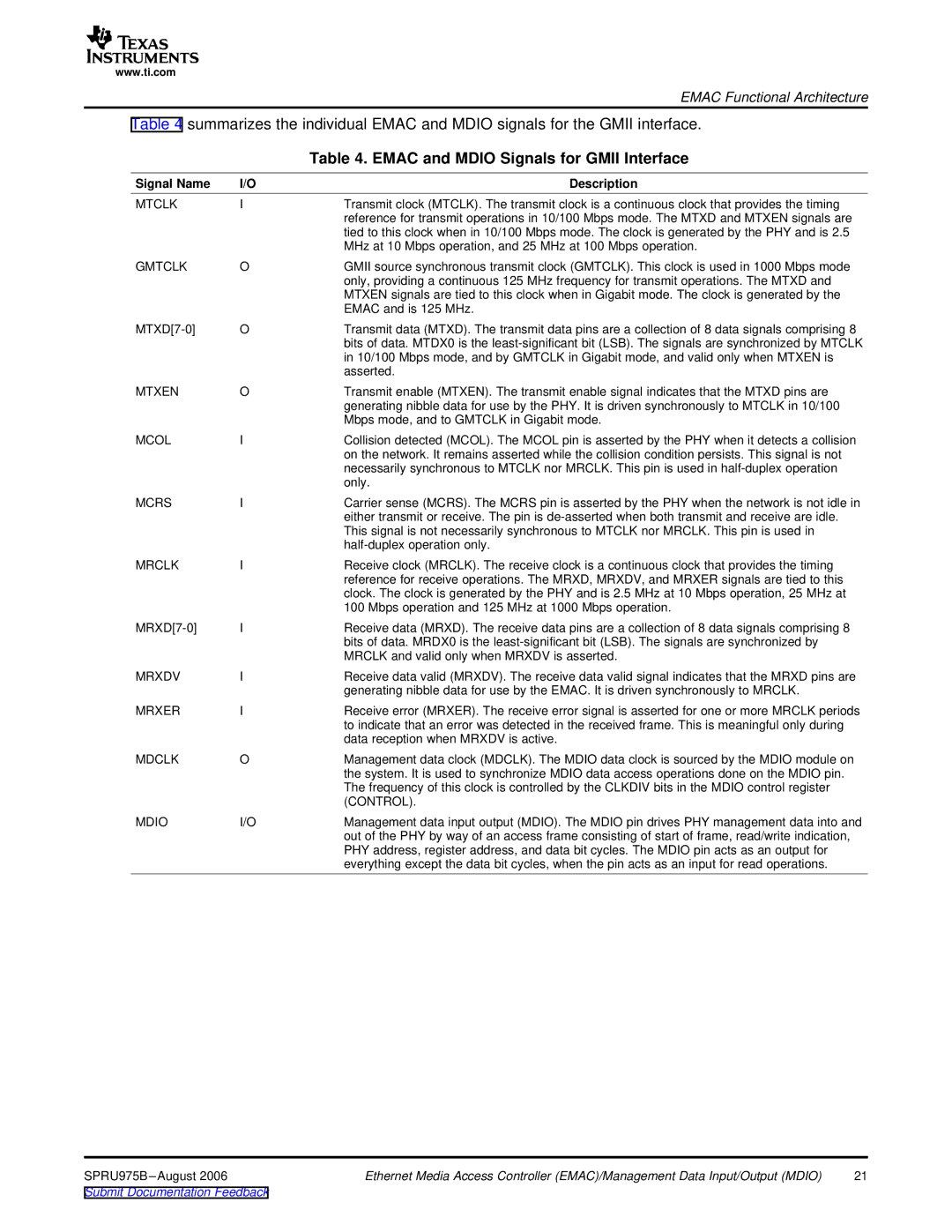
Table 4 summarizes the individual EMAC and MDIO signals for the GMII interface. | ||
|
| Table 4. EMAC and MDIO Signals for GMII Interface |
Signal Name | I/O | Description |
MTCLK | I | Transmit clock (MTCLK). The transmit clock is a continuous clock that provides the timing |
|
| reference for transmit operations in 10/100 Mbps mode. The MTXD and MTXEN signals are |
|
| tied to this clock when in 10/100 Mbps mode. The clock is generated by the PHY and is 2.5 |
|
| MHz at 10 Mbps operation, and 25 MHz at 100 Mbps operation. |
GMTCLK | O | GMII source synchronous transmit clock (GMTCLK). This clock is used in 1000 Mbps mode |
|
| only, providing a continuous 125 MHz frequency for transmit operations. The MTXD and |
|
| MTXEN signals are tied to this clock when in Gigabit mode. The clock is generated by the |
|
| EMAC and is 125 MHz. |
O | Transmit data (MTXD). The transmit data pins are a collection of 8 data signals comprising 8 | |
|
| bits of data. MTDX0 is the |
|
| in 10/100 Mbps mode, and by GMTCLK in Gigabit mode, and valid only when MTXEN is |
|
| asserted. |
MTXEN | O | Transmit enable (MTXEN). The transmit enable signal indicates that the MTXD pins are |
|
| generating nibble data for use by the PHY. It is driven synchronously to MTCLK in 10/100 |
|
| Mbps mode, and to GMTCLK in Gigabit mode. |
MCOL | I | Collision detected (MCOL). The MCOL pin is asserted by the PHY when it detects a collision |
|
| on the network. It remains asserted while the collision condition persists. This signal is not |
|
| necessarily synchronous to MTCLK nor MRCLK. This pin is used in |
|
| only. |
MCRS | I | Carrier sense (MCRS). The MCRS pin is asserted by the PHY when the network is not idle in |
|
| either transmit or receive. The pin is |
|
| This signal is not necessarily synchronous to MTCLK nor MRCLK. This pin is used in |
|
| |
MRCLK | I | Receive clock (MRCLK). The receive clock is a continuous clock that provides the timing |
|
| reference for receive operations. The MRXD, MRXDV, and MRXER signals are tied to this |
|
| clock. The clock is generated by the PHY and is 2.5 MHz at 10 Mbps operation, 25 MHz at |
|
| 100 Mbps operation and 125 MHz at 1000 Mbps operation. |
I | Receive data (MRXD). The receive data pins are a collection of 8 data signals comprising 8 | |
|
| bits of data. MRDX0 is the |
|
| MRCLK and valid only when MRXDV is asserted. |
MRXDV | I | Receive data valid (MRXDV). The receive data valid signal indicates that the MRXD pins are |
|
| generating nibble data for use by the EMAC. It is driven synchronously to MRCLK. |
MRXER | I | Receive error (MRXER). The receive error signal is asserted for one or more MRCLK periods |
|
| to indicate that an error was detected in the received frame. This is meaningful only during |
|
| data reception when MRXDV is active. |
MDCLK | O | Management data clock (MDCLK). The MDIO data clock is sourced by the MDIO module on |
|
| the system. It is used to synchronize MDIO data access operations done on the MDIO pin. |
|
| The frequency of this clock is controlled by the CLKDIV bits in the MDIO control register |
|
| (CONTROL). |
MDIO | I/O | Management data input output (MDIO). The MDIO pin drives PHY management data into and |
|
| out of the PHY by way of an access frame consisting of start of frame, read/write indication, |
|
| PHY address, register address, and data bit cycles. The MDIO pin acts as an output for |
|
| everything except the data bit cycles, when the pin acts as an input for read operations. |
SPRU975B | Ethernet Media Access Controller (EMAC)/Management Data Input/Output (MDIO) | 21 |
Submit Documentation Feedback |
|
|