www.ti.com
|
| EMAC Functional Architecture |
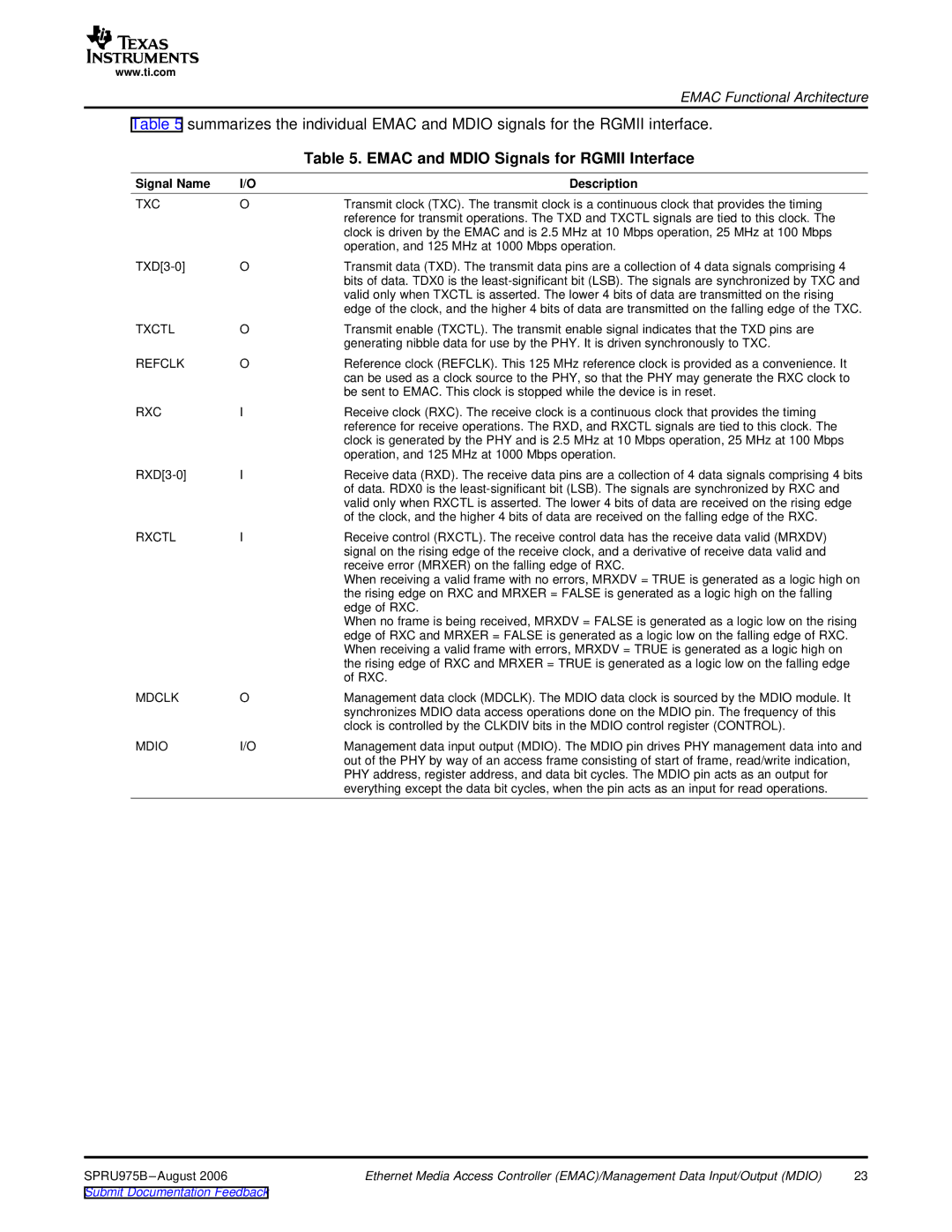
Table 5 summarizes the individual EMAC and MDIO signals for the RGMII interface. | ||
|
| Table 5. EMAC and MDIO Signals for RGMII Interface |
Signal Name | I/O | Description |
TXC | O | Transmit clock (TXC). The transmit clock is a continuous clock that provides the timing |
|
| reference for transmit operations. The TXD and TXCTL signals are tied to this clock. The |
|
| clock is driven by the EMAC and is 2.5 MHz at 10 Mbps operation, 25 MHz at 100 Mbps |
|
| operation, and 125 MHz at 1000 Mbps operation. |
O | Transmit data (TXD). The transmit data pins are a collection of 4 data signals comprising 4 | |
|
| bits of data. TDX0 is the |
|
| valid only when TXCTL is asserted. The lower 4 bits of data are transmitted on the rising |
|
| edge of the clock, and the higher 4 bits of data are transmitted on the falling edge of the TXC. |
TXCTL | O | Transmit enable (TXCTL). The transmit enable signal indicates that the TXD pins are |
|
| generating nibble data for use by the PHY. It is driven synchronously to TXC. |
REFCLK | O | Reference clock (REFCLK). This 125 MHz reference clock is provided as a convenience. It |
|
| can be used as a clock source to the PHY, so that the PHY may generate the RXC clock to |
|
| be sent to EMAC. This clock is stopped while the device is in reset. |
RXC | I | Receive clock (RXC). The receive clock is a continuous clock that provides the timing |
|
| reference for receive operations. The RXD, and RXCTL signals are tied to this clock. The |
|
| clock is generated by the PHY and is 2.5 MHz at 10 Mbps operation, 25 MHz at 100 Mbps |
|
| operation, and 125 MHz at 1000 Mbps operation. |
I | Receive data (RXD). The receive data pins are a collection of 4 data signals comprising 4 bits | |
|
| of data. RDX0 is the |
|
| valid only when RXCTL is asserted. The lower 4 bits of data are received on the rising edge |
|
| of the clock, and the higher 4 bits of data are received on the falling edge of the RXC. |
RXCTL | I | Receive control (RXCTL). The receive control data has the receive data valid (MRXDV) |
|
| signal on the rising edge of the receive clock, and a derivative of receive data valid and |
|
| receive error (MRXER) on the falling edge of RXC. |
|
| When receiving a valid frame with no errors, MRXDV = TRUE is generated as a logic high on |
|
| the rising edge on RXC and MRXER = FALSE is generated as a logic high on the falling |
|
| edge of RXC. |
|
| When no frame is being received, MRXDV = FALSE is generated as a logic low on the rising |
|
| edge of RXC and MRXER = FALSE is generated as a logic low on the falling edge of RXC. |
|
| When receiving a valid frame with errors, MRXDV = TRUE is generated as a logic high on |
|
| the rising edge of RXC and MRXER = TRUE is generated as a logic low on the falling edge |
|
| of RXC. |
MDCLK | O | Management data clock (MDCLK). The MDIO data clock is sourced by the MDIO module. It |
|
| synchronizes MDIO data access operations done on the MDIO pin. The frequency of this |
|
| clock is controlled by the CLKDIV bits in the MDIO control register (CONTROL). |
MDIO | I/O | Management data input output (MDIO). The MDIO pin drives PHY management data into and |
|
| out of the PHY by way of an access frame consisting of start of frame, read/write indication, |
|
| PHY address, register address, and data bit cycles. The MDIO pin acts as an output for |
|
| everything except the data bit cycles, when the pin acts as an input for read operations. |
SPRU975B | Ethernet Media Access Controller (EMAC)/Management Data Input/Output (MDIO) | 23 |
Submit Documentation Feedback |
|
|