8XC196MC, 8XC196MD, 8XC196MH Microcontroller User’ Manual
We Value Your Opinion
Page
8XC196MC, 8XC196MD, 8XC196MH Microcontroller User’s Manual
Intel Corporation
Contents
Chapter Memory Partitions
Contents
8XC196MC, MD, MH USER’S Manual
Application Example
PWM Signals and Registers
Functional Overview Programming the Frequency Generator
Programming the Waveform Generator
Chapter Event Processor Array EPA
Chapter Minimum Hardware Considerations
Chapter Programming the Nonvolatile Memory
Appendix C Registers Glossary Index
Figures
10-5
15-9 Ready Timing Diagram One Wait State 8XC196MH
15-21
Tables
11-12
16-7 Pmode Values
Guide to This Manual
Page
Manual Contents
Chapter Guide to this Manual
Special Operating Modes
Notational Conventions and Terminology
Assert and deassert
Numbers
Related Documents
Application Notes, Application Briefs, and Article Reprints
Handbooks and Product Information
Title Order Number
MCS 96 Microcontroller Datasheets Commercial/Express
MCS 96 Microcontroller Datasheets Automotive
This Page Left Intentionally Blank
Guide to this Manual
This Page Left Intentionally Blank
Technical Support
World Wide Web
Product Literature
Page
Architectural Overview
Page
Microcontroller Features
Typical Applications
Otprom
Features of the 8XC196Mx Product Family
Functional Overview
SIO PWM
CPU
ROM
PTS EPA PWM WDT SIO
RAM
Register File
CPU Control
Register Arithmetic-logic Unit Ralu
Code Execution
Instruction Format
Interrupt Service
Memory Interface Unit
Internal Timing
Clock Circuitry
Internal Peripherals
State Times at Various Frequencies
1 I/O Ports
Serial I/O SIO Port
Frequency Generator
Event Processor Array EPA and Timer/Counters
Pulse-width Modulator PWM
Waveform Generator
Testing the Printed Circuit Board
Watchdog Timer
Reducing Power Consumption
Analog-to-digital Converter
Programming the Nonvolatile Memory
Programming Considerations
Page
Operand Type No. Signed Possible Values Addressing
Overview of the Instruction SET
Operand Type Definitions
Restrictions
SHORT-INTEGER Operands
BIT Operands
Byte Operands
Word Operands
Integer Operands
DOUBLE-WORD Operands
Conditional Jumps
LONG-INTEGER Operands
Converting Operands
Floating Point Operations
Addressing Modes
Indirect Addressing
Direct Addressing
Immediate Addressing
Definition of Temporary Registers
Indirect Addressing with the Stack Pointer
Indexed Addressing
Indirect Addressing with Autoincrement
Short-indexed Addressing
Long-indexed Addressing
Zero-indexed Addressing
Using Registers
Assembly Language Addressing Mode Selections
Software Standards and Conventions
Addressing 32-bit Operands
Linking Subroutines
Software Protection Features and Guidelines
8XC196MC, MD, MH USER’S Manual
Memory Partitions
Page
External Devices Memory or I/O
Memory Partitions
Program and Special-purpose Memory
Device
Program Memory
Memory Map
Description Addressing Modes
Reserved Memory Locations
Special-purpose Memory
Special-purpose Memory Addresses
Interrupt and PTS Vectors
Special-function Registers SFRs
Chip Configuration Bytes CCBs
Security Key
Memory-mapped SFRs
Peripheral SFRs
Port 2 SFRs
EPA and Timer SFRs
Peripheral SFRs 8XC196MC
SFRs
Peripheral SFRs 8XC196MD
Ports 2 and 7 SFRs
Port 1 SFRs
Peripheral SFRs 8XC196MH
Port 0 and 2 SFRs
Serial I/O Port SFRs
Register File Memory Map
Address
Stack Pointer SP
Register File Memory Addresses
General-purpose Register RAM
Device and Hex Address Range Description Addressing Modes
CPU SFRs
CPU Special-function Registers SFRs
Address High Odd Byte Low Even Byte
02FFH 01FFH
Windowing
8XC196MC,MD
00FFH
Bit Function Number
Selecting a Window
WSR
WSR Value for Peripherals
Addressing a Location Through a Window
10. Selecting a Window of the Upper Register File
Base WSR Value WSR Value for
11. Windows
12. Windowed Base Addresses
Peripheral SFRs
2.3 128-byte Windowing Example
2.1 32-byte Windowing Example
2.2 64-byte Windowing Example
Unsupported Locations Windowing Example
Using the Linker Locator to Set Up a Window
?WSR
This listing shows the disassembled code
Windowing and Addressing Modes
LDB WSR, #12H
Page
Standard and PTS Interrupts
Page
Chapter Standard and PTS Interrupts
Overview of Interrupts
Flow Diagram for PTS and Standard Interrupts
Interrupt Signals
Interrupt Signals and Registers
Interrupt and PTS Control and Status Registers
Ptssel
Interrupt Sources and Priorities
Pipend 1FBEH
Ptssrv
Interrupt Sources, Vectors, and Priorities
Interrupt Controller PTS Service
Interrupt Source Mnemonic Name Vector Priority
Unimplemented Opcode
Special Interrupts
External Interrupt Pin
Software Trap
Multiplexed Interrupt Sources
Waveform Generator Protection Circuitry
Flow Diagram for the Ovrtm Interrupt
Interrupt Latency
End-of-PTS Interrupts
Situations that Increase Interrupt Latency
Calculating Latency
Standard Interrupt Latency
Standard Interrupt Response Time PTS Interrupt Latency
Programming the Interrupts
PTS Mode Execution Time in State Times
Execution Times for PTS Cycles
Standard and PTS Interrupts
8XC196MD
Ptssel
8XC196MC
Bit Function
Bit Mnemonic Interrupt Standard Vector
Intmask
COMP2 EPA2 COMP1 EPA1 COMP3 COMP0 EPA0 Ovrtm
COMP2 MC, MD
NMI Extint EPA5
INTMASK1
NMI Extint
NMI Extint SPI COMP3 EPA3 COMP4 EPA4 RI1 RI0 TI1 TI0
8XC196MC 8XC196MD
Pimask
Bit Function Number Mnemonic
Pimask
Modifying Interrupt Priorities
OVRTM1
Standard and PTS Interrupts
Determining the Source of an Interrupt
10. Interrupt Pending Intpend Register
Intpend
11. Interrupt Pending 1 INTPEND1 Register
INTPEND1
12. Peripheral Interrupt Pending Pipend Register
Pipend
Initializing the PTS Control Blocks
Pipend
Specifying the PTS Count
14. PTS Service Ptssrv Register
Ptssrv
Single Transfer Mode
Selecting the PTS Mode
Ptscon
Register Location Function
PTS Single Transfer Mode Control Block
Ptsdst H Ptsdst L Ptssrc H Ptssrc L Ptscon Ptscount
Ptsdst Ptscb +
Standard and PTS Interrupts
Single Transfer Mode Ptscb
Block Transfer Mode
Block Transfer Mode Ptscb
PTS Block Transfer Mode Control Block
Ptsblock Ptscb +
5 A/D Scan Mode
PTS A/D Scan Mode Control Block
A/D Scan Mode Command/Data Table
Address Contents
5.1 A/D Scan Mode Cycles
5.2 A/D Scan Mode Example
PTSPTR2 H = 1FH PTSPTR2 L = AAH
Command/Data Table Example
A/D Scan Mode Ptscb Example
Ptscount = 04H
11. A/D Scan Mode Ptscb Example
5.3 A/D Scan Mode Example
10. Command/Data Table Example
Serial I/O Modes
SA1 SA0 MAJ
PTS Serial I/O Mode Control Block 1 8XC196MC, MD
Ptsvec
SA1
Baud
Epareg
SA0 †
8XC196MC, MD, MH USER’S Manual
Port Mask Register
PTS Serial I/O Mode Control Block 2 8XC196MC, MD
Port Address Pointer high byte
PTSCON1
Data
Rpar
8XC196MC, MD Register Location Function
PTS Serial I/O Mode Control Block
Portreg
8XC196MC, MD, MH USER’S Manual
13. Ssio Transmit Mode PTSCBs
PTSCB1 PTSCB2
Txddone =
Synchronous SIO Receive Mode Example
23. Synchronous SIO Receive Timing
14. Ssio Receive Mode PTSCBs
Clrb Rxddone
Standard and PTS Interrupts
Rxddone =
25. Asynchronous SIO Transmit Timing
15. Asio Transmit Mode PTSCBs
Standard and PTS Interrupts
End-Of-PTS Interrupt Save Critical Data Is PTS
Asynchronous SIO Receive Mode Example
27. Asynchronous SIO Receive Timing
Samptime = 01H
16. Asio Receive Mode PTSCBs
Portreg H = 1FH P2PIN
Standard and PTS Interrupts
End-Of-PTS Interrupt
Ports
Page
Device I/O Ports
I/O Ports Overview
Port Bits Type Direction Associated Peripherals
Standard Input-only Port Pins
INPUT-ONLY Ports 1 MC, MD only
1FDAH MH
Standard Input-only Port Operation
Input-only Port Registers
P1PIN MC, MD
Standard Input-only Port Considerations
Bidirectional Ports 1 MH ONLY, 2, 5, and 7 MD only
Bidirectional Port Pins
Port Pin Special-function Associated Signals
Bidirectional Port Operation
Bidirectional Port Control and Status Registers
Ports
Bidirectional Port Structure
Logic Table for Bidirectional Ports in I/O Mode
Bidirectional Port Pin Configurations
Sfdir
8XC196MC, MD, MH USER’S Manual
Control Register Values for Each Configuration
Bidirectional Port Pin Configuration Example
Port Configuration Example
Bidirectional Port Considerations
HZ1
P5.1/INST
Bidirectional Ports 3 and 4 ADDRESS/DATA BUS
Ports 3 and 4 Pins
Port Pins Special-function
12. Ports 3 and 4 Control and Status Registers
Bidirectional Ports 3 and 4 Address/Data Bus Operation
Address/Data Bus Ports 3 and 4 Structure
Standard OUTPUT-ONLY Port
Using Ports 3 and 4 as I/O
Design Considerations for Ports 3
13. Logic Table for Ports 3 and 4 as Open-drain I/O
Output-only Port Operation
Configuring Output-only Port Pins
14. Standard Output-only Port Pins
15. Output-only Port Control Register
1FC0H
Reset State 0000H
Wgoutput Port Address
OP1 OP0
Reset State 0000H
Wgoutput Port
Page
Serial I/O SIO Port
Page
SIO Block Diagram
Serial I/O SIO Port Functional Overview
Serial Port Signals
Serial I/O Port Signals and Registers
Serial Port Control and Status Registers
P1PIN 1F9FH
P1DIR 1F9BH
P1REG 1F9DH
Serial Port Modes
Synchronous Modes Modes 0
Mode
Mode 0 Timing
Asynchronous Modes Modes 1, 2,
Serial Port Frames for Mode
Mode 2 and 3 Timings
Multiprocessor Communications
Programming the Control Register
Configuring the Serial Port Pins
Programming the Serial Port
SP xCON Address 1F83H, 1F8BH = 0-1 8XC196MH
Bit Function
BV7
Programming the Baud Rate and Clock Source
Clksrc
BV9 BV8
Baudvalue =
Bclk
80CFH
SPxBAUD Values When Using XTAL1 at 16 MHz
Enabling the Serial Port Interrupts
E82BH
RPE/RB8 TXE
Determining Serial Port Status
RPE/RB8
8XC196MC, MD, MH USER’S Manual
Frequency Generator
Page
Chapter Frequency Generator
Frequency Generator Control and Status Registers
Frequency Generator Signal
Port Frequency
Programming the Frequency
Configuring the Output
Programming the Frequency Generator
Freqgen
Application Example
Determining the Current Value of the Down-counter
Freqcnt
Frequency Generator
0FAH
Xmitbuf Dsb Bufsize Block of data to send Shiftreg
Stb temp,freqgen0 Into freq gen
Frequency Generator
Page
Waveform Generator
Page
Chapter Waveform Generator
Waveform Generator Functional Overview
Waveform Generator Block Diagram
Waveform Generator Signals
Waveform Generator Signals and Registers
Waveform Generator Control and Status Registers
Waveform Generator Operation
Timebase Generator
Phase Driver Channels
Control and Protection Circuitry
Register Buffering and Synchronization
Protection Circuitry
Operating Modes
Operation in Center-aligned and Edge-aligned Modes
Register Updates
Event Mode
Step Center-aligned Modes Edge-aligned Modes
Center-aligned Modes
Center-aligned Modes Counter Operation
Center-aligned Modes Output Operation Edge-Aligned Modes
Edge-aligned Modes Counter Operation
Output Configuration
Configuring the Outputs
Programming the Waveform Generator
PE6
Wgoutput Waveform Generator
OP1 OP0 Sync PE7
OP1
8XC196MC, MD, MH USER’S Manual
E0H
Wgprotect
F0H
8XC196MC, MD 8XC196MH Bit Function Number Mnemonic
Reload
Specifying the Carrier Period and Duty Cycle
Wgreload
150 Reload
Wgcomp Address
1FC2H,1FC4H,1FC6H
DT7 DT6 DT5 DT4 DT9 DT8 DT3 DT2 DT1 DT0
Wgcontrol
Wgcounter = Wgreload
Wgcounter
Determining the Waveform GENERATOR’S Status
Enabling the Waveform Generator Interrupts
Xxxxh
Wgcount WGCOUNT=
Design Considerations
Dead Time and Duty Cycle
Wgcomp
Programming Example
Ph3 Dsw P6.4,5 config
Waveform Generator
Temp1,WGOUTPUT0 Now store it Ret
Demo board PI interrupt
Page
Pulse-width Modulator
Page
Chapter PULSE-WIDTH Modulator
PWM Functional Overview
PWM Signals and Registers
PWM Signals
PWM Control and Status Registers
PWM Operation
PEx Pin Output
E6H
Programming the Frequency and Period
FFH
PWM Output Frequencies Fpwm
Pwmperiod
Programming the Duty Cycle
Pwmperiod +
Reading the Current Value of the Down-counter
Sample Calculations
PWM xCONTROL Address 10-3
PWM Output Alternate Functions
PWM Output Alternate Port Function PWM Output Enabled When
Enabling the PWM Outputs
Pwmcount
Waveform Generator Output Configuration Wgoutput Register
D/A Buffer Block Diagram
Generating Analog Outputs
Event Processor Array EPA
Page
Device Capture/Compare Channels Compare-only Channels
EPA Functional Overview
EPA Channels
COMP30
EPA and TIMER/COUNTER Signals and Registers
EPA and Timer/Counter Signals
EPA Control and Status Registers
P0PIN 1FA8H
P1PIN 1FA9H
TIMER2 1F7EH
TIMER/COUNTER Functional Overview
TIMER1 1F7AH
T1RELOAD
EPA Timer/Counters
Cascade Mode Timer 2 Only
Quadrature Clocking Modes
State of Xinternal State of Yinternal Count Direction
T1DIR
Quadrature Mode Timing and Count
EPA Channel Functional Overview
Operating in Capture Mode
A Single EPA Capture/Compare Channel
EPA Simplified Input-capture Structure
EPA Overruns
Action Taken When a Valid Edge Occurs
Overwrite Bit Status Action Taken When a Valid Edge Occurs
EPAxCON.0
Preventing EPA Overruns
Operating in Compare Mode
Generating a Low-speed PWM Output
Generating the Highest-speed PWM Output
Configuring the EPA and Timer/Counter Signals
Programming the EPA and TIMER/COUNTERS
Programming the Timers
T1CONTROL
Prescaler Divisor Resolution †
Clock Source Direction Source
Prescaler Resolution †
T2CONTROL
Mode WGR ROT ON/RT
Example EPA Control Register Settings for Channels 1, 3, or
Programming the Capture/Compare Channels
EPAxCON = 0-1 8XC196MH x = 0-3 8XC196MC x = 0-5 8XC196MD
Capture Mode Event
Compare Mode Action
= 0, 2 = 1, 3
For EPA capture/compare channels 0, 2
EPA xCON Address
= 0, 2
For EPA capture/compare channels 1, 3
Capture Mode on
Compare Mode RT
Comp xCON Address
= 0-3 8XC196MC, MH = 0-5 8XC196MD Reset State 00H
Programming the Compare-only Channels
WGR ROT
Enabling the EPA Interrupts
Determining Event Status
Analog-to-digital Converter
PageNum-38
12.1 A/D Converter Functional Overview
Angnd
Port Pin Signal Description
12.2 A/D Converter Signals and Registers
A/D Converter Pins
A/D Control and Status Registers
12.3 A/D Converter Operation
P1PIN MC,MD
Programming the A/D Converter
Adtest
Programming the A/D Test Register
OFF1 OFF0
Programming the A/D Time Register
Adresult Write
Programming the A/D Command Register
Adtime
Enabling the A/D Interrupt
Adcommand
M1 M0 Mode
ACH3 ACH2 ACH1 ACH0
Adresult Read
Determining A/D Status and Conversion Results
ADRLT90
Designing External Interface Circuitry
Idealized A/D Sampling Circuitry
Minimizing the Effect of High Input Source Resistance
Suggested A/D Input Circuit
Understanding A/D Conversion Errors
Using Mixed Analog and Digital Inputs
12-14
Ideal A/D Conversion Characteristic
10. Actual and Ideal A/D Conversion Characteristics
12-17
11. Terminal-based A/D Conversion Characteristic
Minimum Hardware Considerations
Page
RESET#
Minimum Required Signals
Minimum Connections
Unused Inputs
I/O Port Configuration Guide
Port Where to Find Configuration Information
13.1.2 I/O Port Pin Connections
Minimum Hardware Connections
Applying and Removing Power
Noise Protection Tips
ON-CHIP Oscillator Circuitry
On-chip Oscillator Circuit
External Crystal Connections
Using AN External Clock Source
External Clock Connections
Resetting the Device
Reset Timing Sequence
Rsts
Gencon
Rsts DR0
DRO
Generating an External Reset
Internal Reset Circuitry
10. Minimum Reset Circuit
Issuing an Illegal Idlpd Key Operand
Issuing the Reset RST Instruction
Enabling the Watchdog Timer
Generating Wait States
1EH E1H
Selecting the Watchdog Reset Interval 8XC196MH only
First Byte Second Byte Reset Interval
1EH A1H
Page
Special Operating Modes
Page
Port Pin Signal Type Description
Special Operating Mode Signals and Registers
Operating Mode Control Signals
Clkout
ONCE#
Operating Mode Control and Status Registers
Port Pin Signal Type Description Name
CCR0
P7MODEMD 1FD1H
Reducing Power Consumption
P1MODEMH
P1REG MH 1F9DH
Idle Mode
Clock Control During Power-saving Modes
Powerdown Mode
Enabling and Disabling Powerdown Mode
Generating a Hardware Reset
Entering Powerdown Mode
Exiting Powerdown Mode
Driving the VPP Pin Low
Asserting the External Interrupt Signal
External RC Circuit
Selecting R1 and C1
Typical Voltage on the VPP Pin While Exiting Powerdown
Once Mode
Reserved Test Modes
Page
Interfacing with External Memory
Page
Signal Port Pin Type Description Name
External Memory Interface Signals and Registers
External Memory Interface Signals
ADV#
CCR0.1
Bytes Accessed
BHE# AD0
CCR1.2 Buswidth
EA#
Signal Port Pin
WR#
WRL#
External Memory Interface Registers
WRH#
Register Address Description Mnemonic
P5REG = 11XX Xxxxb
Chip Configuration Registers and Chip Configuration Bytes
BHE#/WRH# †
15-6
LOC1 LOC0
CCR0
LOC1 LOC0 IRC1 IRC0 ALE BW0
IRC2 IRC1 IRC0
ALE
CCR0
BW1 BW0
WDE BW1 IRC2
CCR1
WDE
BUS Width and Multiplexing
CCR1
Multiplexing and Bus Width Options
Buswidth Timing Diagram 8XC196MC, MD
Symbol Definition
Buswidth Signal Timing Definitions
Timing Requirements for Buswidth
15.3.2 16-bit Bus Timings
Timings for 16-bit Buses
15.3.3 8-bit Bus Timings
Wait States Ready Control
Timings for 8-bit Buses
15-18
Ready Timing Diagram One Wait State 8XC196MC, MD
Address Valid to Ready Setup
BUS-CONTROL Modes
Bus-control Mode Bus-control Signals CCR0.3 CCR0.2
Bus-control Modes
Standard Bus-control Mode
BHE# WR# AD0
CS#
ALE OE# WE# RD# WR#
Eprom RAM
Buswidth CS#
OE# WE# RD# WR#
Write Strobe Mode
14. Write Strobe Mode
15 -bit System with Writes to Byte-wide RAMs
OE# OE# WE# RD# WRH# WRL#
Address Valid Strobe Mode
16. Address Valid Strobe Mode
18 -bit System with Flash
Eprom
OE# RD#
Address Valid with Write Strobe Mode
20. Timings of Address Valid with Write Strobe Mode
WRH# WRL# CS#
System BUS AC Timing Specifications
VCC Buswidth
WE# CS#
22. System Bus Timing
External Memory Systems Must Meet These Specifications
Explanation of AC Symbols
AC Timing Symbol Definitions Signals
AC Timing Definitions
Microcontroller Meets These Specifications
Address Setup to ALE/ADV# Low
15-35
Page
Programming Nonvolatile Memory
Page
Programming the Nonvolatile Memory
Programming Methods
Otprom Memory MAP
C196Mx Otprom Memory Map
Security Features
Controlling Access to Internal Memory
Address Range Description Hex
Controlling Access to the Otprom During Programming Modes
Controlling Access to the Otprom During Normal Operation
Memory Protection for Normal Operating Mode
Read Protect Write Protect Protection Status
Security Key
Memory Protection Options for Programming Modes
Pccb CCB
Controlling Fetches from External Memory
Usfr
Uprom Programming Values and Locations for Slave Mode
To set this bit Write this value To this location
PPW
Programming Pulse Width
Ppwvalue
BitBitFunction Number Mnemonic
8XC196MC, MD 8XC196MH Two 250-µs pulses required
Modified QUICK-PULSE Algorithm
Example Ppwvalue Calculations
Ppwvalue =
Modified Quick-pulse Algorithm
Programming Mode Pins
Special Program Port Pin
Cpver
PROG#
AINC#
PACT#
Entering Programming Modes
Selecting the Programming Mode
Pmode Values
Power-up Sequence
Power-up and Power-down Sequences
Power-down Sequence
Slave Programming Mode
Reading the Signature Word and Programming Voltages
Device Signature Word Programming VCC
Slave Programming Circuit and Memory Map
Device Signature Word and Programming Voltages
Location Value
Operating Environment
Slave Programming Mode Memory Map
Description Address Comments
LOC1 LOC0 IRC1 IRC0 WDE BW1 IRC2
CCR1, CCR0
Bit Mnemonic Function
Slave Programming Routines
Address/Command Decoding Routine
Program Word Routine
Program Word Waveform
10. Dump Word Routine
10. Timing Mnemonics
Timing Mnemonics
MnemonicDescription
Auto Programming Circuit and Memory Map
Auto Programming Mode
Mnemonic Description
12. Auto Programming Circuit
Auto Programming Routine
Address Internal Address Using Output from
Address Internal Address Using
11 XC196MC/MD Auto Programming Memory Map
13. Auto Programming Routine
Auto Programming Procedure
ROM-dump Mode
Pccb and Uprom Programming 8XC196MH only
14. Pccb and Uprom Programming Circuit
13. Pccb and Uprom Programming Values
Pins Pccb Programming Uprom Programming
RUN-TIME Programming
PMODE30 0DH
15. Run-time Programming Code Example
Page
Instruction Set Reference
Page
Appendix a Instruction SET Reference
Table A-1. Opcode Map Left Half
Opcode
Table A-1. Opcode Map Right Half
Value of Bits Shifted Off
Table A-2. Processor Status Word PSW Flags
Instruction Quotient Stored Flag Set if Quotient is
Symbol Description
Table A-4. PSW Flag Setting Symbols
Instruction Jumps to Destination if Continues if
Table A-5. Operand Variables
Variable Description
Mnemonic Operation
PSW Flag Settings
Table A-6. Instruction Set
C V VT ST
Dest ← Dest and SRC
Instruction Format
Andb
PTRS, Cntreg
Count
Count ← Count
Count ← Cntreg Loop Srcptr ← Ptrs Dstptr
Dstptr ← Srcptr Ptrs ← Srcptr +
Dest
Clear BYTE. Clears the value
Mnemonic Operation Instruction Format
← Dest MOD SRC
Dest MOD SRC
Djnz Decrement and Jump if not Zero
Djnzw Decrement and Jump if not Zero
Epts
Dpts Disable Peripheral Transaction
Epts Enable Peripheral Transaction
EXT SIGN-EXTEND Integer Into Long
Extb SIGN-EXTEND SHORT-INTEGER Into
Increment BYTE. Increments the value Byte operand by
JGE Jump if Signed Greater than or
JLE Jump if Signed Less than or Equal
Negative flag is set, this instruction adds
JNV Jump if Overflow Flag is Clear
Jnvt Jump if OVERFLOW-TRAP Flag is
JVT Jump if OVERFLOW-TRAP Flag is SET
Load Byte SIGN-EXTENDED. Sign
MUL
Mulb
Mulu
Mulub
Integer operand
SRC, Dest
Dest ← not Dest
Dest ← Dest or SRC
INTMASK1/WSR ← SP
PSW/INTMASK ← SP
SP ← PSW/INTMASK PSW/INTMASK ←
SP ← INTMASK1/WSR INTMASK1 ←
Scall
Wreg, #count
SHR
Range of 0 to 31 1FH, inclusive. If
Shral Arithmetic Right Shift Double
Shrl Logical Right Shift DOUBLE-WORD
Skip
Rightmost operand
SUB
Subc
Subb
Subc Subtract Words with Borrow DEST, SRC
Subcb Subtract Bytes with Borrow DEST, SRC
× Offset + Tbase = Dest
Index and #MASK = Offset
Tijmp TBASE, INDEX, #MASK
XOR
Dest ← Dest XOR SRC
Clrb Notb Negb
Table A-7. Instruction Opcodes
Hex Code Instruction Mnemonic
Decb Extb Incb Shrb Shlb Shrab
Hex Code
Hex Code
8XC196MC, MD, MH USER’S Manual
Dpts Epts
EF Lcall
DIV/DIVB/MUL/MULB Note
Arithmetic Group Direct Immediate Indirect Indexed Mnemonic
Table A-8. Instruction Lengths and Hexadecimal Opcodes
Subc Subcb
Logical Direct Immediate Indirect
Data Direct
Stack Direct Immediate Indirect Indexed Mnemonic
Opcode Length
Jump Direct
Length Opcode
Call Direct Immediate Indirect Indexed Mnemonic
Conditional Jump Direct Immediate
PTS
Shift Mnemonic Direct Immediate Indirect Indexed
Special Mnemonic Direct Immediate Indirect
Mnemonic Direct Immediate Indirect
Normal Autoinc Short Long Reg Mem
Table A-9. Instruction Execution Times in State Times
Arithmetic Group Indirect
Mem Reg
DIV Divb Divu Divub
Mnemonic Direct Immed Normal Autoinc Short Long Reg Mem
Logical
Normal Autoinc Short
Stack Register Indirect
Reg Mem
Autoinc Short Long
Autoinc Short Long Reg
LDB Ldbse Ldbze STB XCH Xchb
Ljmp Sjmp Tijmp
Normal Autoinc Short Long
Call Memory Indirect Indexed Mnemonic Direct
Conditional Jump Mnemonic
Clrc Clrvt Idlpd
Shift Mnemonic Direct
Indirect Indexed
NOP RST Setc Skip
Page
Signal Descriptions
Page
Table B-1. Signal Name Changes
Signal Name Changes
Functional Groupings of Signals
New Name
Table B-2 XC196MC Signals Arranged by Functional Categories
Figure B-1 XC196MC 64-lead Shrink DIP Sdip Package
U8XC196MC
Figure B-2 XC196MC 84-lead Plcc Package
X8XC196MC
Figure B-3 XC196MC 80-lead Shrink EIAJ/QFP Package
Table B-3 XC196MD Signals Arranged by Functional Categories
P7.7/FREQOUT
Figure B-4 XC196MD 84-lead Plcc Package
X8XC196MD
Figure B-5 XC196MD 80-lead Shrink EIAJ/QFP Package
EA# Extint NMI ONCE# RESET# XTAL1 XTAL2
Table B-4 XC196MH Signals Arranged by Functional Categories
P2.7/SCLK1#/BCLK1
Figure B-6 XC196MH 64-lead Shrink DIP Sdip Package
X8XC196MH
Figure B-7 XC196MH 84-lead Plcc Package
Signal Descriptions
Figure B-8 XC196MH 80-lead Shrink EIAJ/QFP Package
Table B-5. Description of Columns of Table B-6
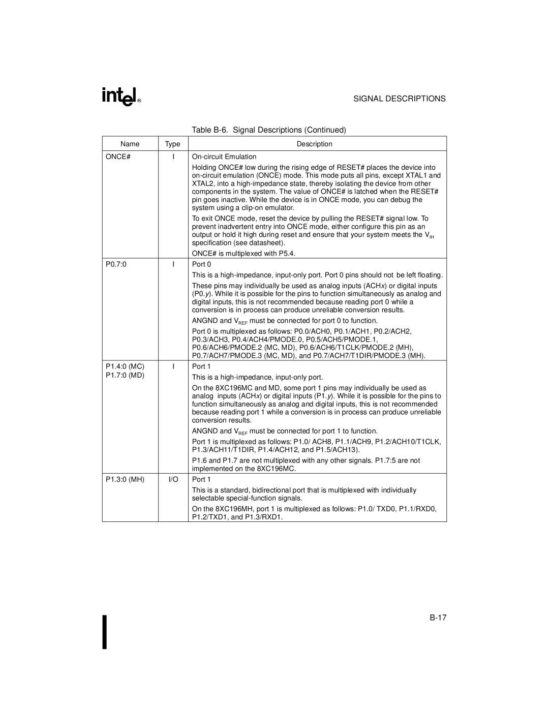
Table B-6. Signal Descriptions
Column Heading Description Name
BCLK10
Buswidth
CCR0.1 CCR1.2
COMP1/P2.5/PACT#, COMP2/P2.6/CPVER, COMP3/P2.7MC, MD
Command that invoked the power-saving mode
System using a clip-on emulator
P5.7/BUSWIDTH
Auto programming
Slave programming
PMODE.30
Programming Start
SCLK10# Shift Clock 0 MH only
Default Conditions
Port Signals Alternate During Upon RESET#
Table B-7. Definition of Status Symbols
Table B-8 XC196MC and MD Default Signal Conditions
Functions RESET# Active
WG3 WK1
NMI WK0 RESET#
WG2 WK1
PWM0 WK0
Port Signals
Table B-9 XC196MH Default Signal Conditions
RESET#
Alternate During Upon
Osc output
Registers
Page
CPU
Table C-1. Modules and Related Registers
8XC196MC, MH, x =
Table C-2. Register Name, Address, and Reset Status
Xxxx EPA4TIME MD
Xxxx EPA2TIME MC, MD
Xxxx EPA3TIME MC, MD
Xxxx EPA5TIME MD
1FFD
P7PIN MD
Xxxx P1REG MH
P5REG MC, MD
Usfr MC, MD
Xxxx TIMER1
TIMER2
Usfr MH Xxxx Watchdog
Adcommand
Adresult Read
Adresult Write
Adtest
Adtime
CCR0
ALE
CCR1
IRC2 IRC1 IRC0
COMPxCON
Comp xCON Address Table C-3 = 0-3 8XC196MC, MH
For EPA capture/compare channels 0, 2
COMPxTIME
Table C-3. COMPxTIME Addresses and Reset Values
Register Address Reset Value
Comp xTIME Address
EPAxCON
EPAxCON Address Table C-4 = 0-1 8XC196MH
= 0-3 8XC196MC x = 0-5 8XC196MD
Table C-4. EPAxCON Addresses and Reset Values
= 0-3 8XC196MC = 0-5 8XC196MD
EPAxTIME
Table C-5. EPAxTIME Addresses and Reset Values
EPA Timer Value
EPAxTIME = 0-1 8XC196MH x = 0-3 8XC196MC x = 0-5 8XC196MD
Freqcnt
Freqgen
Gencon
Intmask
OVRTM†
INTMASK1
Intpend
INTPEND1
Ffffh
Onesreg
Onesreg
One
= 1 MH
Table C-6. PxDIR Addresses and Reset Values
PxDIR
= 2, 5 M
= 1 MH = 2, 5 Mx
Table C-7. PxMODE Addresses and Reset Values
PxMODE
PIN7 PIN6 PIN5 PIN4
Port
Table C-8. Special-function Signals for Ports 1, 2, 5
Pin Special-function Signal
8XC196MC, MD
Table C-9. PxPIN Addresses and Reset Values
PxPIN
PxREG = 2-5 8XC196MC = 2-5, 7 8XC196MD x = 1-5 8XC196MH
Table C-10. PxREG Addresses and Reset Values
PxREG
= 2-5 M
Pimask
Pimask
Pipend
Pipend
PPW
PPW150 Ppwvalue
PSW
PSW
PSE
PSW
Ptssel
Ptssrv
Pwmcount
Pwmperiod
PWMxCONTROL
PWM xCONTROL Address 1FB0H, 1FB2H
SBUFxRX Address 1F80H, 1F88H = 0-1 8XC196MH
SBUFxRX
8XC196MH Data Received Bit
Sbuf xTX Address 1F82H, 1F8AH = 0-1 8XC196MH
SBUFxTX
8XC196MH Data to Transmit Bit
Stack Pointer
150 Stack Pointer
SPxBAUD
SPxCON
SPxCON Address 1F83H, 1F8BH = 0-1 8XC196MH
SPxSTATUS
T1CONTROL
T1RELOAD
Timer 1 Reload Value
T1RELOAD
T2CONTROL
Timer Address 1F7AH
TIMERx
1F7EH
Usfr
Watchdog
Watchdog
0AH
WGCOMPx
Wgcontrol
Wgcounter
Wgoutput Port
Wgoutput Waveform Generator
Wgoutput Waveform Generator
Table C-11. Output Configuration
Output Values Output Polarities WG x#
Wgprotect
Wgreload
Register Mnemonic
WSR
Byte Windows
00E0-00FFH 00C0-00FFH
00E0-00FFH 00C0-00FFH 0080-00FFH Location
PWM0CONTROL 1FB0H 7DH
T2CONTROL 1F7CH 7BH 00FCH 3DH 1EH TIMER1 † 1F7AH 00FAH
1EH 00FAH TIMER2 † 1F7EH 7BH 00FEH 3DH WGCOMP1 1FC2H
PWM1CONTROL 1FB2H 7DH
Zeroreg
Zeroreg
Zero
Page
Glossary
Page
Glossary
Characteristic
DOUBLE-WORD
LONG-INTEGER
LSB
Otprom
PTS
PWM
SFR
Special interrupt
WDT
Page
Index
Page
Index
Index-2
Index-3
Index-4
Index-5
Index-6
Index-7
Index-8
Index-9
Index-10
Index-11
Index-12
Index-13
Index-14