Datasheet Volume One
May
Page
Contents
Package Thermal Specifications
Mechanical Specifications 245 10.2.1
Figures
Tcase 8-Core 135W Thermal Profile 2U
Tables
Core 150W Thermal Profile, Workstation Platform SKU Only
Fault Resilient Booting Output Tri-State Signals
Revision Description Revision Date Number
Initial Release March
Datasheet Volume One
Overview
Introduction
Processor Feature Details
Interfaces
Supported Technologies
System Memory Support
PCI Express
NTB
Direct Media Interface Gen 2 DMI2
Intel QuickPath Interconnect Intel QPI
Link
Power Management Support
Platform Environment Control Interface Peci
Processor Package and Core States
System States Support
Thermal Management Support
Package Summary
Terminology
Intel QuickPath Interconnect
IMC
IIO
IHS
IOV
LLC
Lrdimm
Nctf
Nebs
Related Documents
TDP
Tsod
Udimm
State of Data
Referenced Documents Sheet 2
System Memory Interface
System Memory Technology Support
System Memory Timing Support
PCI Express* Interface
PCI Express* Architecture
PCI Express* Configuration Mechanism
Transaction Layer
Data Link Layer
Physical Layer
1 DMI2 Error Flow
DMI2/PCI Express* Interface
Intel QuickPath Interconnect
Processor/PCH Compatibility Assumptions
Interfaces
Summary of Processor-specific Peci Commands
Command Supported on the Processor
Platform Environment Control Interface Peci
Peci Client Capabilities
Client Command Suite
Processor Interface Tuning and Diagnostics
Thermal Management
Platform Manageability
GetDIB
Minor Revision Supported Command Suite
Device Info
Revision Number
Minor Revision Number Meaning
GetTemp
Client Address Write Length Read Length
Temp70 Temp158
RdPkgConfig
Supported Responses
GetTemp Response Definition
Response Meaning
WrPkgConfig
RdPkgConfig Response Definition
WrPkgConfig Response Definition Sheet 1
Electrical error or AW FCS failure
Package Configuration Capabilities
WrPkgConfig Response Definition Sheet 2
Dram Thermal and Power Optimization Capabilities
Temperature
Dram Power
By power
Dram Rank
Dram Thermal Estimation Configuration Data Read/Write
Limit Data
Limit
Performance
Dram Rank Temperature Write
Dimm Temperature Read
Channel & Dimm Index Decoding
Index Encoding Physical Channel# Physical DIMM#
Dimm Ambient Temperature Write / Read
Dram Channel Temperature Read
DIMM#
Dram Power Info Read
Accumulated Dram Energy Read
Accumulated Dram Energy Data
Dram Power Limit Data Write / Read
Maximum Time
Typical Value
Dram Power Limit Performance Status Read
Dram Powerlimit
Reserved
CPU Thermal and Power Optimization Capabilities
Cpuid
CSR did
CSR Mcaerrsrclog
Read Mode bit Accumulated
Power Limit for
VCC Power
Read status
Read Package Power
Modes Package Power
Indicator Read
Limits For
Package Identifier Read
Processor
Type
Flag
Package Power SKU Unit Read
Max Thread
Power Control Register Unit Calculations
Package Power SKU Read
Unit Field Value Calculation Default Value
Wake on Peci Mode Bit Write / Read
Package Temperature Read
Maximum Package Power Window
Peci Temperature
Per Core DTS Temperature Read
Temperature Target Read
Package Thermal Status Read / Clear
Thermal Averaging Constant Write / Read
Thermally Constrained Time Read
Current Limit Read
4 3 2 1
Power Limit for the VCC Power Plane Write / Read
Accumulated Energy Status Read
Package Power Limits For Multiple Turbo Modes
Control Time Clamp Power Limit
Mode Enable
Package Power Limit Performance Status Read
Window #2 Mode #2 Enable #2
Efficient Performance Indicator Read
Acpi P-T Notify Write & Read
Read Mode bit 11 = ‘0’
Core ID Bit Read Mode bit 11 = ‘1’
Caching Agent TOR Read
Thermal Margin Read
RdIAMSR
Processor ID Enumeration
42. Processor ID Construction Example
11. RdIAMSR Services Summary Sheet 1
10. RdIAMSR Response Definition
RdIAMSR Capabilities
11. RdIAMSR Services Summary Sheet 2
Or ID Address Meaning Sor ID Byte Dword
RdPCIConfig
44. PCI Configuration Address
RdPCIConfigLocal
12. RdPCIConfig Response Definition
Timely fashion. Retry is appropriate
Appropriate
13. RdPCIConfigLocal Response Definition Sheet 1
PCI Configuration Address
0x05 0x02,0x03,0x05 0xe1 Definition
WrPCIConfigLocal
13. RdPCIConfigLocal Response Definition Sheet 2
14. WrPCIConfigLocal Response Definition
Cmd Code
0xe5
Completion
Power-up Sequencing
WrPCIConfigLocal Capabilities
16. Peci Client Response During Power-Up Sheet 1
Client Management
16. Peci Client Response During Power-Up Sheet 2
Device Discovery
Client Addressing
18. Power Impact of Peci Commands vs. C-states
Command Power Impact
States
17. Socket ID Strapping
Processor Reset
System Service Processor SSP Mode Support
BMC Init Mode
Processor Error Handling
Originator Retry and Timeout Policy
Link Init Mode
Multi-Domain Commands
20. Multi-Domain Command Code Reference
Enumerating Peci Client Capabilities
19. Domain ID Definition
Client Responses
Abort FCS
Completion Codes
21. Completion Code Pass/Fail Mask
DTS Temperature Data
Originator Responses
Format
Interpretation
Temperature Filtering
24. Error Codes and Descriptions
Error Code Description
Reserved Values
Datasheet Volume One
Intel Virtualization Technology Intel VT
Intel VT-x Objectives
Intel VT-x Features
Intel VT-d Features Supported
Intel VT-d Objectives
Security Technologies
Intel Virtualization Technology Processor Extensions
Intel Trusted Execution Technology
Intel Trusted Execution Technology Server Extensions
Intel Advanced Encryption Standard Instructions Intel AES-NI
Execute Disable Bit
Intel Turbo Boost Operating Frequency
Intel Intelligent Power Technology
Enhanced Intel SpeedStep Technology
Intel Advanced Vector Extensions Intel AVX
Intel Dynamic Power Technology Intel DPT
Technologies
Acpi States Supported
System States
System States
Package C-State Support Sheet 1
System Memory Power States Sheet 1
Integrated Memory Controller States
Package C-State Support Sheet 2
Core C-State Support
4 DMI2/PCI Express Link States
Intel QuickPath Interconnect States
6 G, S, and C State Combinations
Processor Core/Package Power Management
Low-Power Idle States
Enhanced Intel SpeedStep Technology
Requesting Low-Power Idle States
Idle Power Management Breakdown of the Processor Cores
Core C-states
Core C0 State
Core C1/C1E State
PLVLx to Mwait Conversion
Core C3 State
Core C6 State
Core C7 State
State Auto-Demotion
Package C-States
Coordination of Core Power States at the Package Level
Package C0
Package C1/C1E
Package C-State Core
Package C2 State
Package C3 State
Package C6 State
System Memory Power Management
Package C-State Power Specifications
10. Package C-State Power Specifications
TDP SKUs C1E W C3 W C6 W Core / 6-Core
CKE Power-Down
Self Refresh
Self Refresh Entry
Self Refresh Exit
DMI2/PCI Express* Power Management
Dram I/O Power Management
DLL and PLL Shutdown
100
Package Thermal Specifications
Thermal Specifications
Tcase and DTS Based Thermal Specifications
Temperaturetarget MSR
3.1 8-Core 150W Thermal Specifications
Processor Thermal Profiles
Processor SKU Summary Table
Thermal Management Specifications
Power W Maximum T Case C Maximum Dtsc
Core 150W Thermal Profile, Workstation Platform SKU Only
3.2 8-Core 135W Thermal Specifications
Tcase 8-Core 135W Thermal Specifications 2U
3, 4
Power W Maximum Tcase C Maximum DTS C
Core 135W Thermal Profile U Sheet 1
3.3 8/6-Core 130W Thermal Specifications
Power W Maximum T Case C Maximum DTS C
Core 135W Thermal Profile U Sheet 2
Tcase 8/6-Core 130W Thermal Profile 1U
Power W Maximum Tcase C Maximum DTS C Core
6-Core 130W Thermal Profile U Sheet 1
3.4 6-Core 130W 1S WS Thermal Specifications
Tcase 6-Core 130W 1S WS Thermal Specifications
Power W Maximum T Case C Maximum DTS C Core
6-Core 130W Thermal Profile U Sheet 2
DTS 6-Core 130W 1S WS Thermal Profile
Core 130W 1S WS Thermal Profile Table Sheet 1
3.5 8-Core 115W Thermal Specifications
10. Tcase 8-Core 115W Thermal Specifications 1U
Core 130W 1S WS Thermal Profile Table Sheet 2
10. Tcase 8-Core 115W Thermal Profile 1U
3.6 8/6-Core 95W Thermal Specifications
11 -Core 115W Thermal Profile U
12. Tcase 8/6-Core 95W Thermal Profile 1U
14. DTS 6-Core 95W Thermal Profile 1U
13 /6-Core 95W Thermal Profile U Sheet 1
3.7 8-Core 70W Thermal Specifications
14. Tcase 8-Core 70W Thermal Specifications 1U
13 /6-Core 95W Thermal Profile U Sheet 2
16. DTS 8-Core 70W Thermal Profile 1U
15 -Core 70W Thermal Profile U
3.8 6-Core 60W Thermal Specifications
16. Tcase 6-Core 60W Thermal Specifications 1U
18. DTS 6-Core 60W Thermal Profile 1U
17 -Core 60W Thermal Profile U
3.9 4-Core 130W Thermal Specifications
18. Tcase 4-Core 130W Thermal Specifications 2U
20. DTS 4-Core 130W Thermal Profile 2U
19 -Core 130W Thermal Profile U Sheet 1
3.10 4-Core 130W 1S WS Thermal Specifications
19 -Core 130W Thermal Profile U Sheet 2
21. Tcase 4-Core 130W 1S WS Thermal Profile
3.11 4-Core 95W Thermal Specifications
22. Tcase 4-Core 95W Thermal Specifications 1U
21 -Core 130W 1S WS Thermal Profile Table
23. Tcase 4-Core 95W Thermal Profile 1U
3.12 4/2-Core 80W Thermal Specifications
24. Tcase 4/2-Core 80W Thermal Specifications 1U
23 -Core 95W Thermal Profile U
25. Tcase 4/2-Core 80W Thermal Profile 1U
Maximum Tcase Maximum DTS C Power W Core
25 /2-Core 80W Thermal Profile U Sheet 1
4.1 8-Core LV95W Thermal Specifications
Maximum T Case Maximum DTS C Power W Core
Embedded Server Processor Thermal Profiles
25 /2-Core 80W Thermal Profile U Sheet 2
28. Tcase 8-Core LV95W Thermal Profile, Embedded Server SKU
29. DTS 8-Core LV95W Thermal Profile, Embedded Server SKU
4.2 8-Core LV70W Thermal Specifications
30. Tcase 8-Core LV70W Thermal Profile, Embedded Server SKU
31. DTS 8-Core LV70W Thermal Profile, Embedded Server SKU
32. Case Temperature Tcase Measurement Location
Thermal Metrology
Processor Core Thermal Features
Processor Temperature
Adaptive Thermal Monitor
Frequency/SVID Control
33. Frequency and Voltage Ordering
On-Demand Mode
Prochotn Signal
Clock Modulation
Thermtripn Signal
Integrated Memory Controller IMC Thermal Features
Dram Throttling Options
MEMHOTC01N and MEMHOTC23N Signal
Hybrid Closed Loop Thermal Throttling CLTTHybrid
Integrated Dual SMBus Master Controllers for SMI
System Memory Interface Signals
Signal Name Description
Memory Channel DDR0, DDR1, DDR2, DDR3
PCI Express* Based Interface Signals
PCI Express* Port 1 Signals
PCI Express* Port 2 Signals Sheet 1
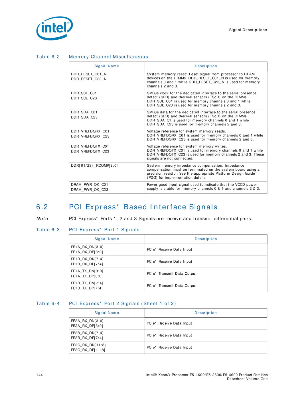
Memory Channel Miscellaneous
PCI Express* Port 2 Signals Sheet 2
PCI Express* Port 3 Signals
PCI Express* Miscellaneous Signals Sheet 1
DMI2/PCI Express* Port 0 Signals
Intel QuickPath Interconnect Signals
Peci Signal
System Reference Clock Signals
Jtag and TAP Signals
Serial VID Interface Svid Signals
Processor Asynchronous Sideband and Miscellaneous Signals
13. Svid Signals
14. Processor Asynchronous Sideband Signals Sheet 1
14. Processor Asynchronous Sideband Signals Sheet 2
Processor Power and Ground Supplies
14. Processor Asynchronous Sideband Signals Sheet 3
15. Miscellaneous Signals
16. Power and Ground Signals Sheet 1
16. Power and Ground Signals Sheet 2
152
Processor Signaling
System Memory Interface Signal Groups
PCI Express* Signals
3 DMI2/PCI Express* Signals
Platform Environmental Control Interface Peci
System Reference Clocks BCLK0/1DP, BCLK0/ 1DN
Input Device Hysteresis
Jtag and Test Access Port TAP Signals
Processor Sideband Signals
Power, Ground and Sense Signals
PLL Power Supply
Power and Ground Lands
Power Number Comments Ground Lands
Decoupling Guidelines
Voltage Identification VID
Svid Commands
SetVID Fast Command
SetVID Slow Command
SetVID-Decay Command
Svid Power State Functions SetPS
VR Power-State Transitions
Svid Voltage Rail Addressing
Svid Address Usage
PWM Address HEX Processor
159
Signal Group Summary
Reserved or Unused Signals
Signal Description Buffer Types Sheet 1
Signal Description
Signal Description Buffer Types Sheet 2
Signal Groups Sheet 1
Signal Groups Sheet 2
Signal Groups Sheet 3
Serial VID Interface Svid Signals
Processor Asynchronous Sideband Signals
Miscellaneous Signals
Power-On Configuration POC Options
Signals with On-Die Termination
Power-On Configuration Option Lands
Signal Name Pull Up /Pull Rail Value Units Down
Fault Resilient Booting FRB
Fault Resilient Booting Output Tri-State Signals
Output Tri-State Signal Groups Signals
Mixing Processors
Symbol Parameter Min Max Unit
Flexible Motherboard Guidelines FMB
Absolute Maximum and Minimum Ratings
Processor Absolute Minimum and Maximum Ratings
Storage Conditions Specifications
10. Storage Condition Ratings
DC Specifications
Voltage and Current Specifications
11. Voltage Specification
Symbol Parameter Voltage Min Typ Max Unit Plane
VCC VID
12. Processor Current Specifications
Parameter Symbol Processor TDP / Core Count
Max a Definition
Core/6-core
13 /6 Core Processor VCC Static and Transient Tolerance
CC a
ICC a
VID 3,4,5,6 100 105 110 115 120 125 130 135 140 145 150
174
VCC Overshoot Specifications
15. VCC Overshoot Specifications Sheet 1
Symbol Parameter Min Max Units
Die Voltage Validation
Signal DC Specifications
15. VCC Overshoot Specifications Sheet 2
16. DDR3 and DDR3L Signal DC Specifications Sheet 1
16. DDR3 and DDR3L Signal DC Specifications Sheet 2
Reference Clock Signal
Command Signals
Control Signals
17. Peci DC Specifications
18. System Reference Clock BCLK0/1 DC Specifications
19. SMBus DC Specifications Sheet 1
Symbol Definition and Conditions Min Max Units
19. SMBus DC Specifications Sheet 2
20. Jtag and TAP Signals DC Specifications
21. Serial VID Interface Svid DC Specifications Sheet 1
Symbol Parameter Min Typ Max Units
21. Serial VID Interface Svid DC Specifications Sheet 2
22. Processor Asynchronous Sideband DC Specifications
CMOS1.05v Signals
Open Drain Cmos Odcmos Signals
PCI Express* DC Specifications
3.2 DMI2/PCI Express* DC Specifications
Intel QuickPath Interconnect DC Specifications
Reset and Miscellaneous Signal DC Specifications
Stable
VRB-Differential
Vcross MAX = 550mV
Vcross MIN = 250mV
Signal Quality
1 DDR3 Signal Quality Specifications
2 I/O Signal Quality Specifications
Intel QuickPath Interconnect Signal Quality Specifications
Input Reference Clock Signal Quality Specifications
24. Processor I/O Overshoot/Undershoot Specifications
Overshoot/Undershoot Tolerance
Reading Overshoot/Undershoot Specification Tables
Overshoot/Undershoot Pulse Duration
Activity Factor
11. Maximum Acceptable Overshoot/Undershoot Waveform
Listing by Land Name
Land Name Sheet 1
Land Name Sheet 2
Land Name Land No Buffer Type Direction
Land Name Sheet 3
Land Name Sheet 4
Land Name Sheet 5
Land Name Sheet 6
Land Name Sheet 7
Land Name Sheet 8
Land Name Sheet 9
Land Name Sheet 10
Land Name Sheet 11
Land Name Sheet 12
Land Name Sheet 13
Land Name Sheet 14
Land Name Sheet 15
Land Name Sheet 16
Land Name Sheet 17
Land Name Sheet 18
Land Name Sheet 19
Land Name Sheet 20
Land Name Sheet 21
Land Name Sheet 22
Land Name Sheet 23
Land Name Sheet 24
Land Name Sheet 25
Land Name Sheet 26
Land Name Sheet 27
Land Name Sheet 28
Land Name Sheet 29
Land Name Sheet 30
Land Name Sheet 31
Land Name Sheet 32
Land Name Sheet 33
Land Name Sheet 34
VCCD01
VCCD23
Land Name Sheet 35
Land Name Sheet 36
Land Name Sheet 37
Land Name Sheet 38
Land Name Sheet 39
Land Name Sheet 40
Land Name Sheet 41
Land Name Sheet 42
Land Name Sheet 43
Land Name Sheet 44
Land Name Sheet 45
Land Name Sheet 46
Land Name Sheet 47
Land Name Sheet 48
Vtta
Vttd
Land Name Sheet 49
Listing by Land Number
Land Number Sheet 1
Land Number Sheet 2
Land No Land Name Buffer Type Direction
Land Number Sheet 3
Land Number Sheet 4
Land Number Sheet 5
Land Number Sheet 6
Land Number Sheet 7
Land Number Sheet 8
Land Number Sheet 9
Land Number Sheet 10
Land Number Sheet 11
Land Number Sheet 12
Land Number Sheet 13
Land Number Sheet 14
Land Number Sheet 15
Land Number Sheet 16
Land Number Sheet 17
Land Number Sheet 18
Land Number Sheet 19
Land Number Sheet 20
Land Number Sheet 21
Land Number Sheet 22
Land Number Sheet 23
Land Number Sheet 24
Land Number Sheet 25
Land Number Sheet 26
Land Number Sheet 27
Land Number Sheet 28
Land Number Sheet 29
Land Number Sheet 30
Land Number Sheet 31
Land Number Sheet 32
Land Number Sheet 33
Land Number Sheet 34
Land Number Sheet 35
Land Number Sheet 36
Land Number Sheet 37
Land Number Sheet 38
Land Number Sheet 39
Land Number Sheet 40
Land Number Sheet 41
Land Number Sheet 42
Land Number Sheet 43
Land Number Sheet 44
Land Number Sheet 45
Land Number Sheet 46
Land Number Sheet 47
Land Number Sheet 48
236
Processor Package Assembly Sketch
Package Mechanical Drawing
238
Processor Package Drawing Sheet 1
Processor Package Drawing Sheet 2
Package Loading Specifications
Package Insertion Specifications
Processor Component Keep-Out Zones
Package Handling Guidelines
Processor Mass Specification
Processor Materials
Processor Markings
Processor Materials
Boxed Processor Specifications
Available Boxed Thermal Solution Configurations
244
Mechanical Specifications
STS200P and STS200PNRW 25.5 mm Tall Passive Heat Sinks
Motherboard Keepout Zones 1
246
Boxed Processor Specifications
Motherboard Keepout Zones 2
Boxed Processor Motherboard Keepout Zones 3
248
Motherboard Keepout Zones 4
TOP Surface of Motherboard
Boxed Processor Heat Sink Volumetric 1
250
Heat Sink Volumetric 2
Specifications
Processor
Boxed Processor
10.4-Pin Fan Cable Connector For Active Heat Sink
11 -Pin Base Baseboard Fan Header For Active Heat Sink
Fan Power Supply STS200C
21,000 25,000 28,000
Boxed Processor Cooling Requirements
Boxed Processor Contents
Boxed Processor
258