Note
Undefined Registers
Channel Voltage
Offset Calibration
Registers
A different gain value is required for voltage and current output operation.
The registers from C016 through FE16 are undefined.
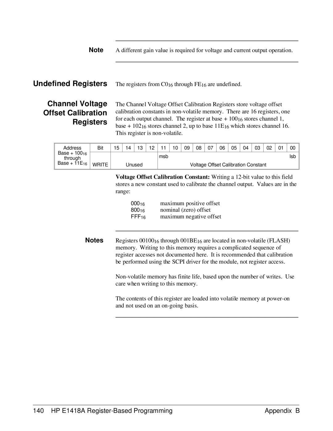
The Channel Voltage Offset Calibration Registers store voltage offset calibration constants in
Address | Bit | 15 | 14 | 13 | 12 | 11 | 10 | 09 | 08 | 07 | 06 | 05 | 04 | 03 | 02 | 01 | 00 |
Base + 10016 |
|
|
|
|
|
|
|
|
|
|
|
|
|
|
|
|
|
|
|
|
|
| msb |
|
|
|
|
|
|
|
|
| lsb | ||
through |
|
|
|
|
|
|
|
|
|
|
|
|
|
| |||
|
|
|
|
|
|
|
|
|
|
|
|
|
|
|
|
| |
Base + 11E16 | WRITE |
| Unused |
|
|
| Voltage Offset Calibration Constant | ||||||||||
|
|
|
|
| |||||||||||||
|
|
|
|
|
|
|
|
|
|
|
|
|
|
|
|
|
|
|
|
|
|
|
|
|
|
|
|
|
|
|
|
|
|
|
|
Voltage Offset Calibration Constant: Writing a
00016 maximum positive offset
80016 nominal (zero) offset
FFF16 maximum negative offset
Notes Registers 0010016 through 001BE16 are located in
The contents of this register are loaded into volatile memory at
140 HP E1418A | Appendix B |
