Maps and Registers | FPGA Registers |
|
|
Bit | Description | Default | Access |
4 | Enable reference clock CLK3_A | 02 | r/w |
| 0: Disabled |
|
|
| 1: Enabled |
|
|
5 | Enable reference clock CLK3_B | 02 | r/w |
| 0: Disabled |
|
|
| 1: Enabled |
|
|
6 | Selects if clock divider is bypassed | 12 | r/w |
| 0: Divide clock |
|
|
| 1: Bypass divider |
|
|
7 | Selection between pulse/clock on | 12 | r/w |
| REF_CLK output signal |
|
|
0: Pulse enabled
1: Pulse disabled
Reference Clock Divider Registers
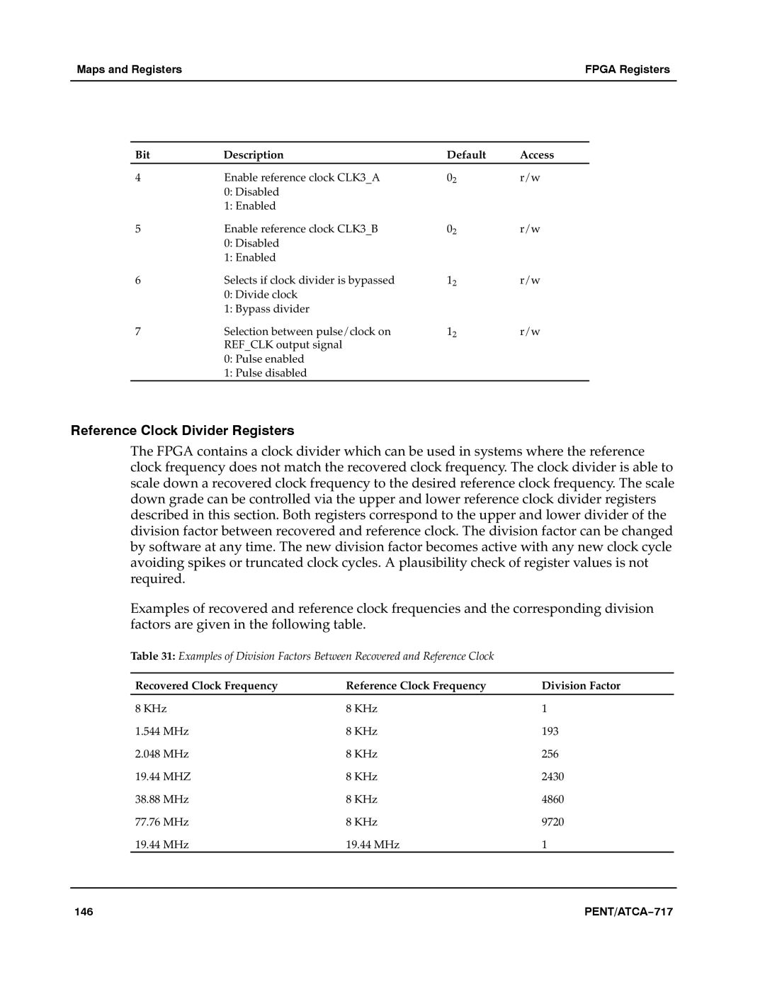
The FPGA contains a clock divider which can be used in systems where the reference clock frequency does not match the recovered clock frequency. The clock divider is able to scale down a recovered clock frequency to the desired reference clock frequency. The scale down grade can be controlled via the upper and lower reference clock divider registers described in this section. Both registers correspond to the upper and lower divider of the division factor between recovered and reference clock. The division factor can be changed by software at any time. The new division factor becomes active with any new clock cycle avoiding spikes or truncated clock cycles. A plausibility check of register values is not required.a
Examples of recovered and reference clock frequencies and the corresponding division factors are given in the following table.a
Table 31: Examples of Division Factors Between Recovered and Reference Clock
Recovered Clock Frequency | Reference Clock Frequency | Division Factor |
8 KHz | 8 KHz | 1a |
1.544 MHz | 8 KHz | 193 |
2.048 MHz | 8 KHz | 256 |
19.44 MHZ | 8 KHz | 2430 |
38.88 MHz | 8 KHz | 4860 |
77.76 MHz | 8 KHz | 9720 |
19.44 MHz | 19.44 MHz | 1a |
146 | PENT/ATCA−717 |
