FPGA Registers | Maps and Registers |
|
|
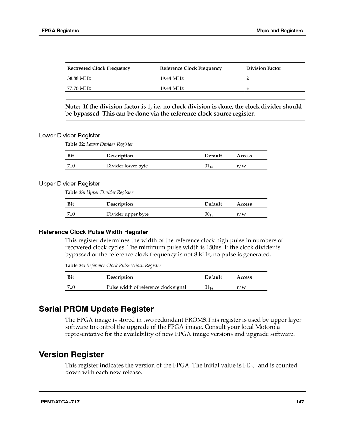
Recovered Clock Frequency | Reference Clock Frequency | Division Factor |
|
38.88 MHz | 19.44 MHz | 2 |
|
77.76 MHz | 19.44 MHz | 4 |
|
|
|
|
|
Note:aIf the division factor is 1, i.e. no clock division is done, the clock divider should be bypassed. This can be done via the reference clock source register.a
Lower Divider Register
Table 32: Lower Divider Register
Bit | Description | Default | Access |
7..0 | Divider lower byte | 0116 | r/w |
Upper Divider Register
Table 33: Upper Divider Register
Bit | Description | Default | Access |
7..0 | Divider upper byte | 0016 | r/w |
Reference Clock Pulse Width Register
This register determines the width of the reference clock high pulse in numbers of recovered clock cycles. The minimum pulse width is 150ns. If the clock divider is bypassed or the reference clock frequency is not 8 kHz, no pulse is generated.a
Table 34: Reference Clock Pulse Width Register
Bit | Description | Default | Access |
7..0 | Pulse width of reference clock signal | 0116 | r/w |
Serial PROM Update Register
The FPGA image is stored in two redundant PROMS.This register is used by upper layer software to control the upgrade of the FPGA image. Consult your local Motorola representative for the availability of new FPGA image versions and upgrade software.a
Version Register
This register indicates the version of the FPGA. The initial value is FE16a and is counted down with each new release.a
PENT/ATCA−717 | 147 |