FPGA Registers | Maps and Registers |
|
|
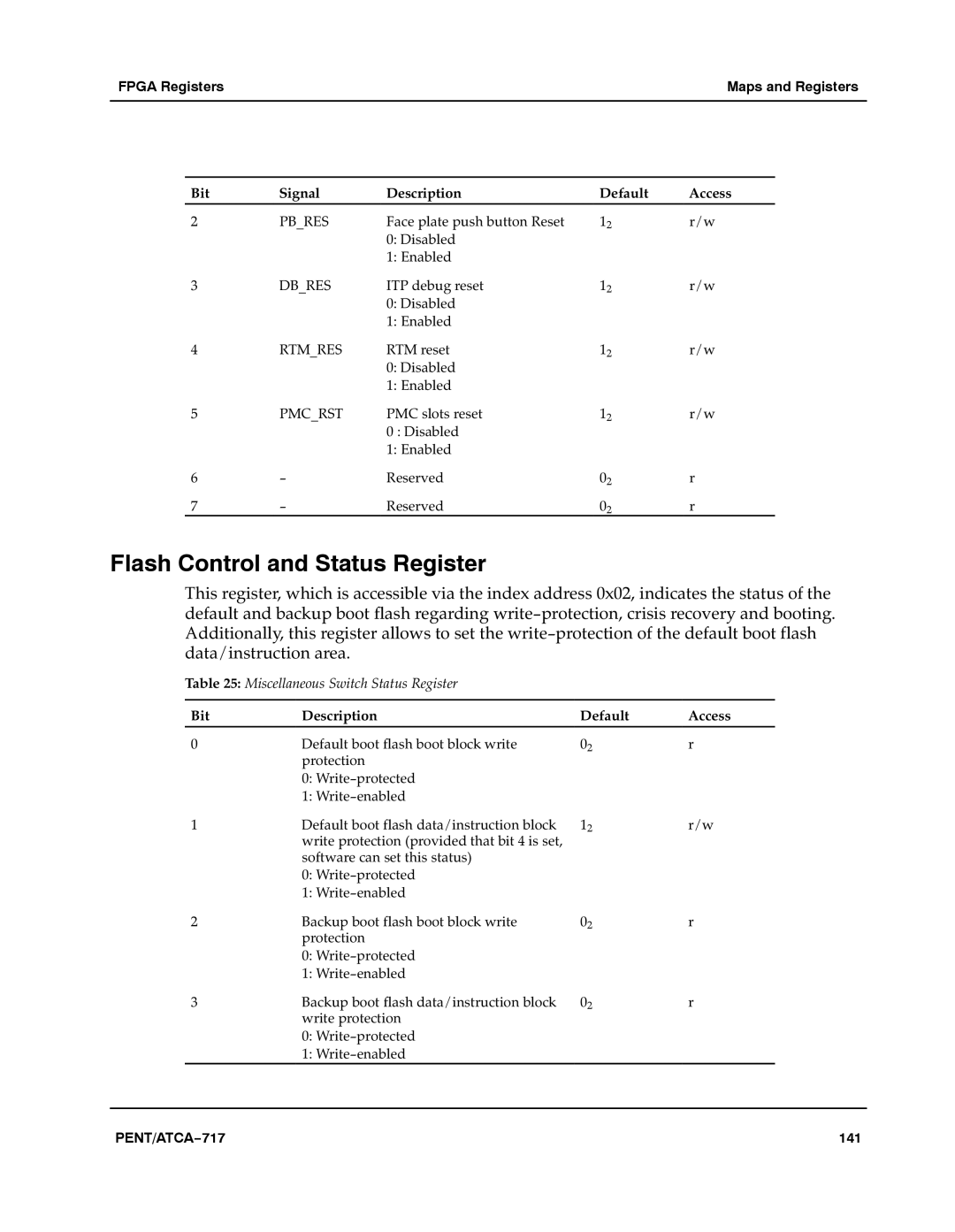
Bit | Signal | Description | Default | Access |
2 | PB_RES | Face plate push button Reset | 12 | r/w |
|
| 0: Disabled |
|
|
|
| 1: Enabled |
|
|
3 | DB_RES | ITP debug reset | 12 | r/w |
|
| 0: Disabled |
|
|
|
| 1: Enabled |
|
|
4 | RTM_RES | RTM reset | 12 | r/w |
|
| 0: Disabled |
|
|
|
| 1: Enabled |
|
|
5 | PMC_RSTa | PMC slots reset | 12 | r/w |
|
| 0 : Disabled |
|
|
|
| 1: Enabled |
|
|
6 | − | Reserved | 02 | r |
7 | − | Reserved | 02 | r |
Flash Control and Status Register
This register, which is accessible via the index address 0x02, indicates the status of the default and backup boot flash regarding write−protection, crisis recovery and booting. Additionally, this register allows to set the write−protection of the default boot flash data/instruction area.aa
Table 25: Miscellaneous Switch Status Register
Bit | Description | Default | Access |
0 | Default boot flash boot block write | 02 | r |
| protection |
|
|
| 0: Write−protected |
|
|
| 1: Write−enabled |
|
|
1 | Default boot flash data/instruction block | 12 | r/w |
| write protection (provided that bit 4 is set, |
|
|
| software can set this status) |
|
|
| 0: Write−protected |
|
|
| 1: Write−enabled |
|
|
2 | Backup boot flash boot block write | 02 | r |
| protection |
|
|
| 0: Write−protected |
|
|
| 1: Write−enabled |
|
|
3 | Backup boot flash data/instruction block | 02 | r |
| write protection |
|
|
0: | Write−protected |
1: | Write−enabled |
PENT/ATCA−717 | 141 |