|
|
|
|
|
|
|
|
|
|
|
| CY7C67300 | |||
|
|
|
|
|
|
|
|
|
|
|
|
|
|
|
|
|
|
|
|
|
|
|
|
|
|
|
|
|
|
|
|
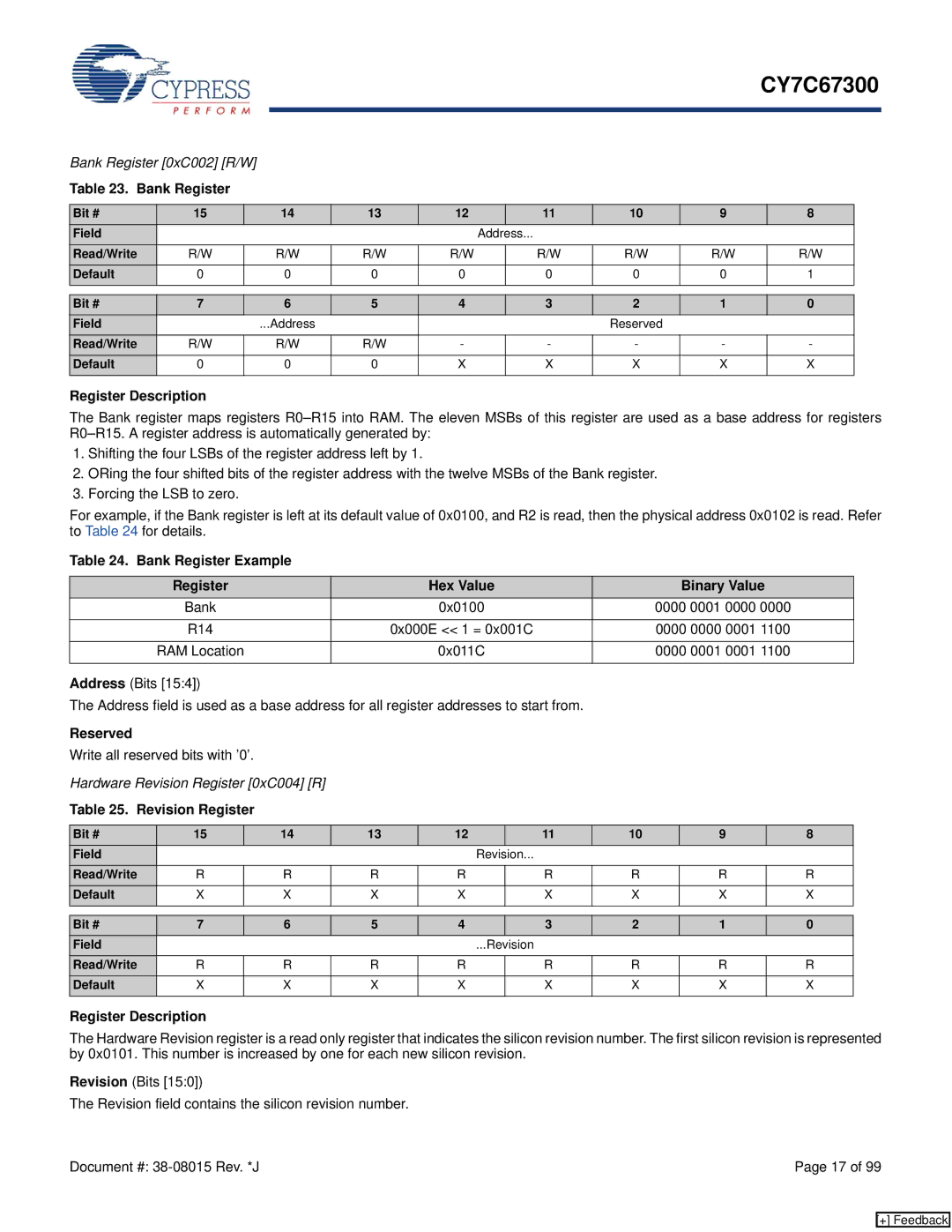
Bank Register [0xC002] [R/W] |
|
|
|
|
|
|
|
|
|
|
|
|
| ||
Table 23. Bank Register |
|
|
|
|
|
|
|
|
|
|
|
|
| ||
|
|
|
|
|
|
|
|
|
|
|
|
|
| ||
Bit # | 15 |
| 14 | 13 | 12 |
| 11 | 10 | 9 |
| 8 |
|
| ||
Field |
|
|
|
|
|
|
| Address... |
|
|
|
|
|
| |
Read/Write | R/W |
|
|
| R/W | R/W | R/W |
| R/W | R/W | R/W |
| R/W |
|
|
Default | 0 |
| 0 | 0 | 0 |
| 0 | 0 | 0 |
| 1 |
|
| ||
|
|
|
|
|
|
|
|
|
|
|
|
|
|
|
|
Bit # | 7 |
| 6 | 5 | 4 |
| 3 | 2 | 1 |
| 0 |
|
| ||
Field |
|
| ...Address |
|
|
|
| Reserved |
|
|
|
|
| ||
Read/Write | R/W |
|
|
| R/W | R/W | - |
| - | - | - |
| - |
|
|
Default | 0 |
| 0 | 0 | X |
| X | X | X |
| X |
|
| ||
|
|
|
|
|
|
|
|
|
|
|
|
|
|
|
|
Register Description
The Bank register maps registers
1.Shifting the four LSBs of the register address left by 1.
2.ORing the four shifted bits of the register address with the twelve MSBs of the Bank register.
3.Forcing the LSB to zero.
For example, if the Bank register is left at its default value of 0x0100, and R2 is read, then the physical address 0x0102 is read. Refer to Table 24 for details.
Table 24. Bank Register Example
| Register |
|
|
| Hex Value |
|
|
| Binary Value |
| |||
| Bank |
|
|
| 0x0100 |
|
| 0000 0001 0000 0000 |
| ||||
|
|
|
|
|
|
|
|
|
|
|
|
|
|
| R14 |
|
| 0x000E << 1 = 0x001C |
|
| 0000 0000 0001 1100 |
| |||||
|
|
|
|
|
|
|
|
|
|
|
|
|
|
| RAM Location |
|
|
| 0x011C |
|
| 0000 0001 0001 1100 |
| ||||
|
|
|
|
|
|
|
|
|
|
|
|
|
|
Address (Bits [15:4]) |
|
|
|
|
|
|
|
|
|
|
| ||
The Address field is used as a base address for all register addresses to start from. |
|
|
|
|
| ||||||||
Reserved |
|
|
|
|
|
|
|
|
|
|
|
|
|
Write all reserved bits with ’0’. |
|
|
|
|
|
|
|
|
|
|
| ||
Hardware Revision Register [0xC004] [R] |
|
|
|
|
|
|
|
|
|
| |||
Table 25. Revision Register |
|
|
|
|
|
|
|
|
|
|
| ||
|
|
|
|
|
|
|
|
|
|
|
|
|
|
Bit # | 15 |
| 14 | 13 |
| 12 |
| 11 | 10 |
| 9 |
| 8 |
Field |
|
|
|
|
| Revision... |
|
|
|
|
|
| |
Read/Write | R |
| R | R |
| R |
| R | R |
| R |
| R |
Default | X |
| X | X |
| X |
| X | X |
| X |
| X |
|
|
|
|
|
|
|
|
|
|
|
|
|
|
Bit # | 7 |
| 6 | 5 |
| 4 |
| 3 | 2 |
| 1 |
| 0 |
Field |
|
|
|
|
| ...Revision |
|
|
|
|
|
| |
Read/Write | R |
| R | R |
| R |
| R | R |
| R |
| R |
Default | X |
| X | X |
| X |
| X | X |
| X |
| X |
|
|
|
|
|
|
|
|
|
|
|
|
|
|
Register Description
The Hardware Revision register is a read only register that indicates the silicon revision number. The first silicon revision is represented by 0x0101. This number is increased by one for each new silicon revision.
Revision (Bits [15:0])
The Revision field contains the silicon revision number.
Document #: | Page 17 of 99 |
[+] Feedback