CY7C67300
External Memory Interface
External Memory Interface Features
■Supports
■SRAM or ROM can be used for code or data space
■Direct addressing of SRAM or ROM
■Two external memory mapped page registers
External Memory Access Strobes
Access to external memory is sampled asynchronously on the rising edge of strobes with a minimum of one wait state cycle. Up to seven wait state cycles may be inserted for external memory access. Each additional wait state cycle stretches the external memory access time by 21 ns (you must be running in internal memory when changing wait states). An external memory device with 12 ns access time is necessary to support 48 MHz code execution.
Page Registers
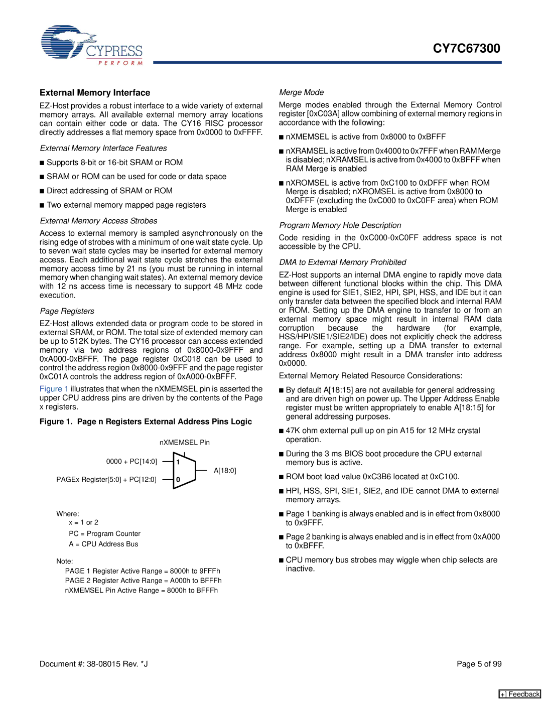
Figure 1 illustrates that when the nXMEMSEL pin is asserted the upper CPU address pins are driven by the contents of the Page x registers.
Figure 1. Page n Registers External Address Pins Logic
| nXMEMSEL Pin | |||||
0000 + PC[14:0] |
|
| 1 |
|
| A[18:0] |
|
|
|
| |||
|
|
|
| |||
|
|
| ||||
PAGEx Register[5:0] + PC[12:0] |
|
| 0 |
|
| |
|
|
|
| |||
|
|
|
|
| ||
|
|
|
| |||
Where:
x = 1 or 2
PC = Program Counter
A = CPU Address Bus
Note:
PAGE 1 Register Active Range = 8000h to 9FFFh PAGE 2 Register Active Range = A000h to BFFFh nXMEMSEL Pin Active Range = 8000h to BFFFh
Merge Mode
Merge modes enabled through the External Memory Control register [0xC03A] allow combining of external memory regions in accordance with the following:
■nXMEMSEL is active from 0x8000 to 0xBFFF
■nXRAMSEL is active from 0x4000 to 0x7FFF when RAM Merge is disabled; nXRAMSEL is active from 0x4000 to 0xBFFF when RAM Merge is enabled
■nXROMSEL is active from 0xC100 to 0xDFFF when ROM Merge is disabled; nXROMSEL is active from 0x8000 to 0xDFFF (excluding the 0xC000 to 0xC0FF area) when ROM Merge is enabled
Program Memory Hole Description
Code residing in the
DMA to External Memory Prohibited
External Memory Related Resource Considerations:
■By default A[18:15] are not available for general addressing and are driven high on power up. The Upper Address Enable register must be written appropriately to enable A[18:15] for general addressing purposes.
■47K ohm external pull up on pin A15 for 12 MHz crystal operation.
■During the 3 ms BIOS boot procedure the CPU external memory bus is active.
■ROM boot load value 0xC3B6 located at 0xC100.
■HPI, HSS, SPI, SIE1, SIE2, and IDE cannot DMA to external memory arrays.
■Page 1 banking is always enabled and is in effect from 0x8000 to 0x9FFF.
■Page 2 banking is always enabled and is in effect from 0xA000 to 0xBFFF.
■CPU memory bus strobes may wiggle when chip selects are inactive.
Document #: | Page 5 of 99 |
[+] Feedback