CY7C67300
IDE Timing
The IDE interface supports PIO mode
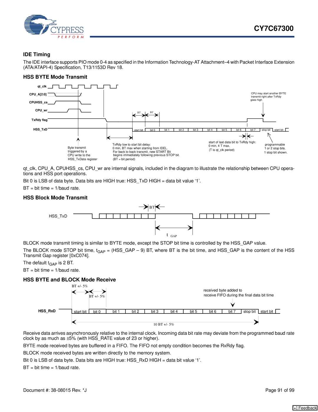
HSS BYTE Mode Transmit
qt_clk
CPU_A[2:0] 
CPUHSS_cs
CPU_wr
TxRdy flag
HSS_TxD
CPU may start another BYTE transmit right after TxRdy goes high
BT BT
start bit |
|
|
|
|
|
|
|
|
|
|
|
| start bit |
|
|
|
|
|
|
|
|
|
|
|
|
|
| ||
|
|
|
|
|
|
|
|
|
|
|
|
| ||
bit 0 | bit 1 | bit 2 | bit 3 | bit 4 | bit 5 | bit 6 |
| bit 7 | stop bit |
| ||||
|
|
|
|
|
|
|
|
|
|
|
|
|
|
|
|
|
|
|
|
|
|
|
|
|
|
|
|
|
|
|
|
|
|
|
|
|
|
|
|
|
|
|
|
|
Byte transmit triggered by a CPU write to the HSS_TxData register
TxRdy low to start bit delay:
0 min, BT max when starting from IDEL. For back to back transmit, new START Bit begins immediately following previous STOP bit.
(BT = bit period)
start of last data bit to TxRdy high: 0 min, 4 T max.
(T is qt_clk period)
programmable
1 or 2 stop bits.
1 stop bit shown.
qt_clk, CPU_A, CPUHSS_cs, CPU_wr are internal signals, included in the diagram to illustrate the relationship between CPU opera- tions and HSS port operations.
Bit 0 is LSB of data byte. Data bits are HIGH true: HSS_TxD HIGH = data bit value ‘1’. BT = bit time = 1/baud rate.
HSS Block Mode Transmit
![]() BT
BT![]()
HSS_TxD
t GAP
BLOCK mode transmit timing is similar to BYTE mode, except the STOP bit time is controlled by the HSS_GAP value.
The BLOCK mode STOP bit time, tGAP = (HSS_GAP – 9) BT, where BT is the bit time, and HSS_GAP is the content of the HSS Transmit Gap register [0xC074].
The default tGAP is 2 BT. BT = bit time = 1/baud rate.
HSS BYTE and BLOCK Mode Receive
HSS_RxD
BT +/- 5% |
|
|
|
|
|
| received byte added to |
|
| |
|
|
|
|
|
|
|
|
| ||
| BT +/- 5% |
|
|
|
|
| receive FIFO during the final data bit time | |||
start bit | bit 0 | bit 1 | bit 2 | bit 3 | bit 4 | bit 5 | bit 6 | bit 7 | stop bit | start bit |
|
|
|
| 10 BT +/- 5% |
|
|
|
|
| |
Receive data arrives asynchronously relative to the internal clock. Incoming data bit rate may deviate from the programmed baud rate clock by as much as ±5% (with HSS_RATE value of 23 or higher).
BYTE mode received bytes are buffered in a FIFO. The FIFO not empty condition becomes the RxRdy flag. BLOCK mode received bytes are written directly to the memory system.
Bit 0 is LSB of data byte. Data bits are HIGH true: HSS_RxD HIGH = data bit value ‘1’. BT = bit time = 1/baud rate.
Document #: | Page 91 of 99 |
[+] Feedback