|
|
|
|
|
|
|
|
|
|
|
|
| CY7C67300 | ||||
|
|
|
|
|
|
|
|
|
|
|
|
|
|
|
|
|
|
|
|
|
|
|
|
|
|
|
|
|
|
|
|
|
|
| |
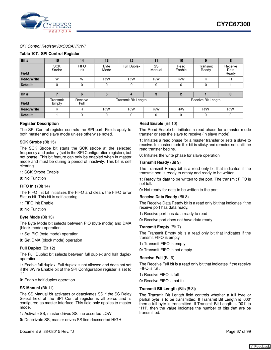
SPI Control Register [0xC0CA] [R/W] |
|
|
|
|
|
|
|
|
|
|
|
|
| ||||
Table 107. SPI Control Register |
|
|
|
|
|
|
|
|
|
|
|
|
| ||||
|
|
|
|
|
|
|
|
|
|
|
|
|
|
|
| ||
Bit # | 15 | 14 | 13 |
| 12 |
| 11 | 10 |
| 9 |
| 8 |
|
|
| ||
| SCK |
|
| FIFO | Byte |
| Full Duplex |
| SS | Read |
| Transmit |
| Receive |
|
| |
Field | Strobe |
|
| Init | Mode |
|
|
| Manual | Enable |
| Ready |
| Data |
| ||
|
|
|
|
|
|
|
|
|
|
|
|
| Ready |
| |||
Read/Write | W |
|
| W | R/W |
| R/W |
| R/W | R/W |
| R |
| R |
|
| |
Default | 0 | 0 | 0 |
| 0 |
| 0 | 0 |
| 0 |
| 1 |
|
|
| ||
|
|
|
|
|
|
|
|
|
|
|
|
|
|
|
|
|
|
Bit # | 7 | 6 | 5 |
| 4 |
| 3 | 2 |
| 1 |
| 0 |
|
|
| ||
Field | Transmit | Receive |
| Transmit Bit Length |
|
| Receive Bit Length |
| |||||||||
Empty |
|
| Full |
|
|
|
|
|
|
|
|
|
|
|
|
| |
Read/Write | R |
|
| R | R/W |
| R/W |
| R/W | R/W |
| R/W |
| R/W |
|
|
|
Default | 1 | 0 | 0 |
| 0 |
| 0 | 0 |
| 0 |
| 0 |
|
|
| ||
|
|
|
|
|
|
|
|
|
|
|
|
|
|
|
|
|
|
Register Description
The SPI Control register controls the SPI port. Fields apply to both master and slave mode unless otherwise noted.
SCK Strobe (Bit 15)
The SCK Strobe bit starts the SCK strobe at the selected frequency and polarity (set in the SPI Configuration register), but not phase. This bit feature can only be enabled when in master mode and must be during a period of inactivity. This bit is self clearing.
1:SCK Strobe Enable
0:No Function
FIFO Init (Bit 14)
The FIFO Init bit initializes the FIFO and clears the FIFO Error Status bit. This bit is self clearing.
1:FIFO Init Enable
0:No Function
Byte Mode (Bit 13)
The Byte Mode bit selects between PIO (byte mode) and DMA (block mode) operation.
1:Set PIO (byte mode) operation
0:Set DMA (block mode) operation
Full Duplex (Bit 12)
The Full Duplex bit selects between full duplex and half duplex operation.
1:Enable full duplex. Full duplex is not allowed and does not set if the 3Wire Enable bit of the SPI Configuration register is set to ‘1’
0:Enable half duplex operation
SSManual (Bit 11)
The SS Manual bit activates or deactivates SS if the SS Delay Select field of the SPI Control register is all zeros and is configured as master interface. This field only applies to master mode.
1:Activate SS, master drives SS line asserted LOW
0:Deactivate SS, master drives SS line deasserted HIGH
Read Enable (Bit 10)
The Read Enable bit initiates a read phase for a master mode transfer or sets the slave to receive (in slave mode).
1:Initiates a read phase for a master transfer or sets a slave to receive. In master mode this bit is sticky and remains set until the read transfer begins.
0:Initiates the write phase for slave operation
Transmit Ready (Bit 9)
The Transmit Ready bit is a read only bit that indicates if the transmit port is ready to empty and ready to be written.
1:Ready for data to be written to the port. The transmit FIFO is not full.
0:Not ready for data to be written to the port
Receive Data Ready (Bit 8)
The Receive Data Ready bit is a read only bit that indicates if the receive port has data ready.
1:Receive port has data ready to read
0:Receive port does not have data ready
Transmit Empty (Bit 7)
The Transmit Empty bit is a read only bit that indicates if the transmit FIFO is empty.
1:Transmit FIFO is empty
0:Transmit FIFO is not empty
Receive Full (Bit 6)
The Receive Full bit is a read only bit that indicates if the receive FIFO is full.
1:Receive FIFO is full
0:Receive FIFO is not full
Transmit Bit Length (Bits [5:3])
The Transmit Bit Length field controls whether a full byte or partial byte is to be transmitted. If Transmit Bit Length is ‘000’ then a full byte is transmitted. If Transmit Bit Length is ‘001’ to ‘111’, then the value indicates the number of bits that are be transmitted.
Document #: | Page 67 of 99 |
[+] Feedback