|
|
|
|
|
|
|
|
| CY7C67300 | |||
|
|
|
|
|
|
|
|
|
|
|
|
|
|
|
|
|
|
|
|
|
|
|
|
| |
GPIO Control Register [0xC006] [R/W] |
|
|
|
|
|
|
|
| ||||
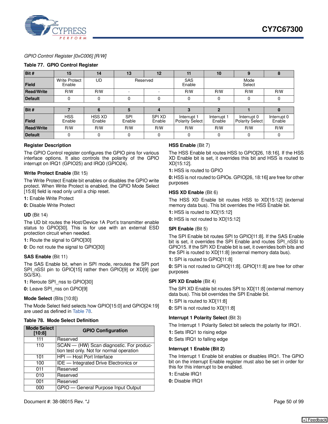
Table 77. GPIO Control Register |
|
|
|
|
|
|
|
| ||||
|
|
|
|
|
|
|
|
|
|
| ||
Bit # | 15 | 14 | 13 | 12 | 11 | 10 | 9 | 8 |
|
| ||
Field | Write Protect |
|
| UD | Reserved | SAS |
| Mode |
|
|
| |
Enable |
|
|
|
|
| Enable |
| Select |
|
|
| |
Read/Write | R/W |
|
| R/W | - | - | R/W | R/W | R/W | R/W |
|
|
Default | 0 | 0 | 0 | 0 | 0 | 0 | 0 | 0 |
|
| ||
|
|
|
|
|
|
|
|
|
|
|
|
|
Bit # | 7 | 6 | 5 | 4 | 3 | 2 | 1 | 0 |
|
| ||
Field | HSS | HSS XD | SPI | SPI XD | Interrupt 1 | Interrupt 1 | Interrupt 0 | Interrupt 0 |
|
| ||
Enable | Enable | Enable | Enable | Polarity Select | Enable | Polarity Select | Enable |
| ||||
Read/Write | R/W |
|
| R/W | R/W | R/W | R/W | R/W | R/W | R/W |
|
|
Default | 0 | 0 | 0 | 0 | 0 | 0 | 0 | 0 |
|
| ||
|
|
|
|
|
|
|
|
|
|
|
|
|
Register Description
The GPIO Control register configures the GPIO pins for various interface options. It also controls the polarity of the GPIO interrupt on IRQ1 (GPIO25) and IRQ0 (GPIO24).
Write Protect Enable (Bit 15)
The Write Protect Enable bit enables or disables the GPIO write protect. When Write Protect is enabled, the GPIO Mode Select [15:8] field is read only until a chip reset.
1:Enable Write Protect
0:Disable Write Protect
UD (Bit 14)
The UD bit routes the Host/Device 1A Port’s transmitter enable status to GPIO[30]. This is for use with an external ESD protection circuit when needed.
1:Route the signal to GPIO[30]
0: Do not route the signal to GPIO[30]
SAS Enable (Bit 11)
The SAS Enable bit, when in SPI mode, reroutes the SPI port SPI_nSSI pin to GPIO[15] rather then GPIO[9] or XD[9] (per SG/SX).
1:Reroute SPI_nss to GPIO[30]
0:Leave SPI_nss on GPIO[9]
Mode Select (Bits [10:8])
The Mode Select field selects how GPIO[15:0] and GPIO[24:19] are used as defined in Table 78.
Table 78. Mode Select Definition
Mode Select | GPIO Configuration | |
[10:8] | ||
| ||
111 | Reserved | |
110 | SCAN — (HW) Scan diagnostic. For produc- | |
| tion test only. Not for normal operation | |
101 | HPI — Host Port Interface | |
100 | IDE — Integrated Drive Electronics or | |
011 | Reserved | |
010 | Reserved | |
001 | Reserved | |
000 | GPIO — General Purpose Input Output |
HSS Enable (Bit 7)
The HSS Enable bit routes HSS to GPIO[26, 18:16]. If the HSS XD Enable bit is set, it overrides this bit and HSS is routed to XD[15:12].
1:HSS is routed to GPIO
0:HSS is not routed to GPIOs. GPIO[26, 18:16] are free for other purposes
HSS XD Enable (Bit 6)
The HSS XD Enable bit routes HSS to XD[15:12] (external memory data bus). This bit overrides the HSS Enable bit.
1:HSS is routed to XD[15:12]
0:HSS is not routed to XD[15:12]
SPI Enable (Bit 5)
The SPI Enable bit routes SPI to GPIO[11:8]. If the SAS Enable bit is set, it overrides the SPI Enable and routes SPI_nSSI to GPIO15. If the SPI XD Enable bit is set, it overrides both bits and the SPI is routed to XD[11:8] (external memory data bus).
1:SPI is routed to GPIO[11:8]
0:SPI is not routed to GPIO[11:8]. GPIO[11:8] are free for other purposes
SPI XD Enable (Bit 4)
The SPI XD Enable bit routes SPI to XD[11:8] (external memory data bus). This bit overrides the SPI Enable bit.
1:SPI is routed to XD[11:8]
0:SPI is not routed to XD[11:8]
Interrupt 1 Polarity Select (Bit 3)
The Interrupt 1 Polarity Select bit selects the polarity for IRQ1.
1:Sets IRQ1 to rising edge
0:Sets IRQ1 to falling edge
Interrupt 1 Enable (Bit 2)
The Interrupt 1 Enable bit enables or disables IRQ1. The GPIO bit on the interrupt Enable register must also be set in order for this for this interrupt to be enabled.
1:Enable IRQ1
0:Disable IRQ1
Document #: | Page 50 of 99 |
[+] Feedback