CY7C67300
Booster Interface
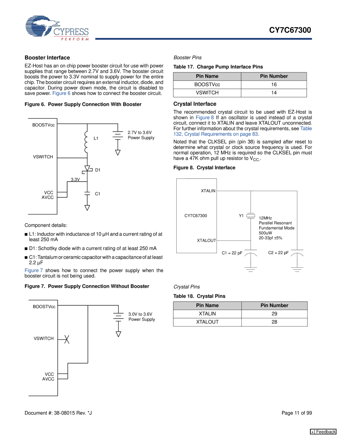
Figure 6. Power Supply Connection With Booster
Booster Pins
Table 17. Charge Pump Interface Pins
Pin Name | Pin Number |
BOOSTVcc | 16 |
|
|
VSWITCH | 14 |
|
|
Crystal Interface
BOOSTVcc
VSWITCH
L1
D1
2.7V to 3.6V Power Supply
The recommended crystal circuit to be used with
Noted that the CLKSEL pin (pin 38) is sampled after reset to determine what crystal or clock source frequency is used. For normal operation, 12 MHz is required so the CLKSEL pin must have a 47K ohm pull up resistor to VCC..
Figure 8. Crystal Interface
VCC AVCC
C1
XTALIN
CY7C67300
Y1
12MHz
Component details:
■ L1: Inductor with inductance of 10 µH and a current rating of at |
least 250 mA |
■ D1: Schottky diode with a current rating of at least 250 mA |
XTALOUT
Parallel Resonant Fundamental Mode 500uW
■ C1: Tantalum or ceramic capacitor with a capacitance of at least |
2.2 µF |
Figure 7 shows how to connect the power supply when the booster circuit is not being used.
Figure 7. Power Supply Connection Without Booster
BOOSTVcc
3.0V to 3.6V
Power Supply
C1 = 22 pF |
|
|
|
|
|
| C2 = 22 pF |
|
|
|
|
|
| ||
|
|
|
|
|
|
|
|
|
|
|
|
|
|
|
|
|
|
|
|
|
|
|
|
Crystal Pins
Table 18. Crystal Pins
Pin Name | Pin Number |
XTALIN | 29 |
|
|
XTALOUT | 28 |
|
|
VSWITCH
VCC
AVCC
Document #: | Page 11 of 99 |
[+] Feedback
