CY7C67300
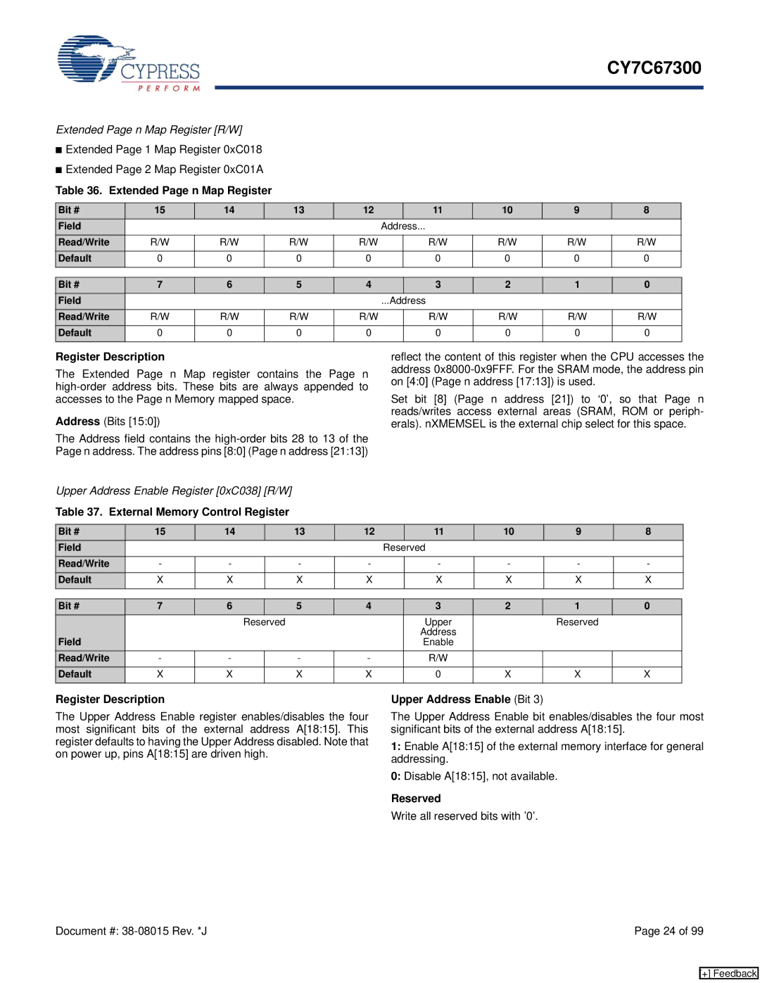
Extended Page n Map Register [R/W]
■Extended Page 1 Map Register 0xC018
■Extended Page 2 Map Register 0xC01A
Table 36. Extended Page n Map Register
Bit # | 15 | 14 | 13 | 12 |
| 11 | 10 | 9 | 8 |
Field |
|
|
|
| Address... |
|
|
| |
Read/Write | R/W | R/W | R/W | R/W |
| R/W | R/W | R/W | R/W |
Default | 0 | 0 | 0 | 0 |
| 0 | 0 | 0 | 0 |
|
|
|
|
|
|
|
|
|
|
Bit # | 7 | 6 | 5 | 4 |
| 3 | 2 | 1 | 0 |
Field |
|
|
|
| ...Address |
|
|
| |
Read/Write | R/W | R/W | R/W | R/W |
| R/W | R/W | R/W | R/W |
Default | 0 | 0 | 0 | 0 |
| 0 | 0 | 0 | 0 |
|
|
|
|
|
|
|
|
|
|
Register Description
The Extended Page n Map register contains the Page n
Address (Bits [15:0])
The Address field contains the
Upper Address Enable Register [0xC038] [R/W]
Table 37. External Memory Control Register
reflect the content of this register when the CPU accesses the address
Set bit [8] (Page n address [21]) to ‘0’, so that Page n reads/writes access external areas (SRAM, ROM or periph- erals). nXMEMSEL is the external chip select for this space.
Bit # | 15 | 14 | 13 | 12 |
| 11 | 10 | 9 | 8 |
Field |
|
|
|
| Reserved |
|
|
| |
Read/Write | - | - | - | - |
| - | - | - | - |
Default | X | X | X | X |
| X | X | X | X |
|
|
|
|
|
|
|
|
|
|
Bit # | 7 | 6 |
| 5 | 4 | 3 | 2 | 1 | 0 |
|
|
| Reserved |
| Upper |
| Reserved |
| |
Field |
|
|
|
|
| Address |
|
|
|
|
|
|
|
| Enable |
|
|
| |
Read/Write | - | - |
| - | - | R/W |
|
|
|
Default | X | X |
| X | X | 0 | X | X | X |
|
|
|
|
|
|
|
|
|
|
Register Description
The Upper Address Enable register enables/disables the four most significant bits of the external address A[18:15]. This register defaults to having the Upper Address disabled. Note that on power up, pins A[18:15] are driven high.
Upper Address Enable (Bit 3)
The Upper Address Enable bit enables/disables the four most significant bits of the external address A[18:15].
1:Enable A[18:15] of the external memory interface for general addressing.
0:Disable A[18:15], not available.
Reserved
Write all reserved bits with ’0’.
Document #: | Page 24 of 99 |
[+] Feedback