|
|
|
|
|
|
|
|
|
|
|
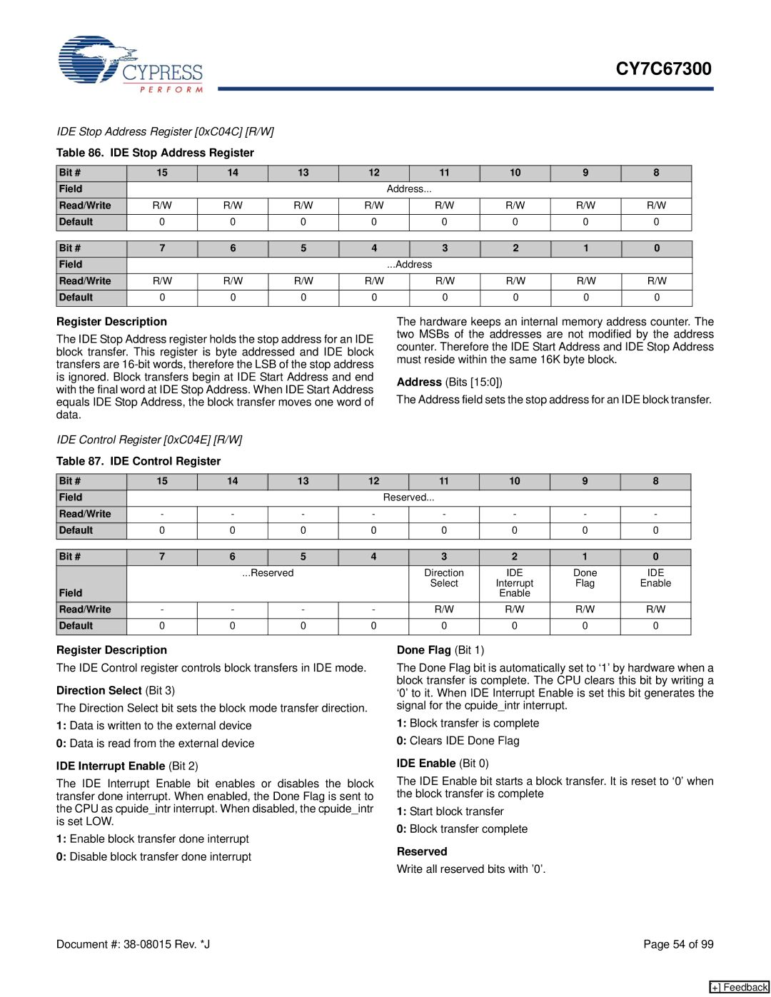
| CY7C67300 | |||
|
|
|
|
|
|
|
|
|
|
|
|
|
|
|
|
|
|
|
|
|
|
|
|
|
|
|
|
|
|
| |
IDE Stop Address Register [0xC04C] [R/W] |
|
|
|
|
|
|
|
|
|
| |||||
Table 86. IDE Stop Address Register |
|
|
|
|
|
|
|
|
|
| |||||
|
|
|
|
|
|
|
|
|
|
|
|
|
| ||
Bit # | 15 | 14 |
| 13 | 12 |
| 11 | 10 | 9 |
| 8 |
|
| ||
Field |
|
|
|
|
|
|
| Address... |
|
|
|
|
|
| |
Read/Write | R/W |
|
| R/W |
| R/W | R/W |
| R/W | R/W | R/W |
| R/W |
|
|
Default | 0 | 0 |
| 0 | 0 |
| 0 | 0 | 0 |
| 0 |
|
| ||
|
|
|
|
|
|
|
|
|
|
|
|
|
|
|
|
Bit # | 7 | 6 |
| 5 | 4 |
| 3 | 2 | 1 |
| 0 |
|
| ||
Field |
|
|
|
|
|
|
| ...Address |
|
|
|
|
|
| |
Read/Write | R/W |
|
| R/W |
| R/W | R/W |
| R/W | R/W | R/W |
| R/W |
|
|
Default | 0 | 0 |
| 0 | 0 |
| 0 | 0 | 0 |
| 0 |
|
| ||
|
|
|
|
|
|
|
|
|
|
|
|
|
|
|
|
Register Description
The IDE Stop Address register holds the stop address for an IDE block transfer. This register is byte addressed and IDE block transfers are
IDE Control Register [0xC04E] [R/W]
Table 87. IDE Control Register
The hardware keeps an internal memory address counter. The two MSBs of the addresses are not modified by the address counter. Therefore the IDE Start Address and IDE Stop Address must reside within the same 16K byte block.
Address (Bits [15:0])
The Address field sets the stop address for an IDE block transfer.
Bit # | 15 | 14 | 13 | 12 |
| 11 | 10 | 9 | 8 |
Field |
|
|
|
| Reserved... |
|
|
| |
Read/Write | - | - | - | - |
| - | - | - | - |
Default | 0 | 0 | 0 | 0 |
| 0 | 0 | 0 | 0 |
|
|
|
|
|
|
|
|
|
|
Bit # | 7 | 6 |
| 5 | 4 | 3 | 2 | 1 | 0 |
|
|
| ...Reserved |
| Direction | IDE | Done | IDE | |
Field |
|
|
|
|
| Select | Interrupt | Flag | Enable |
|
|
|
|
|
| Enable |
|
| |
Read/Write | - | - |
| - | - | R/W | R/W | R/W | R/W |
Default | 0 | 0 |
| 0 | 0 | 0 | 0 | 0 | 0 |
|
|
|
|
|
|
|
|
|
|
Register Description
The IDE Control register controls block transfers in IDE mode.
Direction Select (Bit 3)
The Direction Select bit sets the block mode transfer direction.
1:Data is written to the external device
0:Data is read from the external device
IDE Interrupt Enable (Bit 2)
The IDE Interrupt Enable bit enables or disables the block transfer done interrupt. When enabled, the Done Flag is sent to the CPU as cpuide_intr interrupt. When disabled, the cpuide_intr is set LOW.
1:Enable block transfer done interrupt
0:Disable block transfer done interrupt
Done Flag (Bit 1)
The Done Flag bit is automatically set to ‘1’ by hardware when a block transfer is complete. The CPU clears this bit by writing a ‘0’ to it. When IDE Interrupt Enable is set this bit generates the signal for the cpuide_intr interrupt.
1:Block transfer is complete
0:Clears IDE Done Flag
IDE Enable (Bit 0)
The IDE Enable bit starts a block transfer. It is reset to ‘0’ when the block transfer is complete
1:Start block transfer
0:Block transfer complete
Reserved
Write all reserved bits with ’0’.
Document #: | Page 54 of 99 |
[+] Feedback