CY7C67300
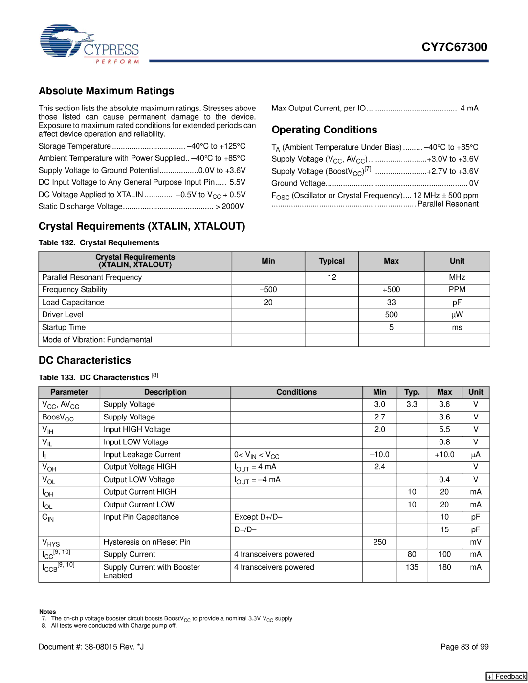
Absolute Maximum Ratings
This section lists the absolute maximum ratings. Stresses above those listed can cause permanent damage to the device. Exposure to maximum rated conditions for extended periods can affect device operation and reliability.
Storage Temperature ..................................
Ambient Temperature with Power Supplied..
Supply Voltage to Ground Potential | ..................0.0V to +3.6V | |
DC Input Voltage to Any General Purpose Input Pin | ..... 5.5V | |
DC Voltage Applied to XTALIN | ||
Static Discharge Voltage | > 2000V | |
Max Output Current, per IO .......................................... 4 mA
Operating Conditions
TA (Ambient Temperature Under Bias) | ......... |
Supply Voltage (VCC, AVCC) | +3.0V to +3.6V |
Supply Voltage (BoostVCC)[7] | +2.7V to +3.6V |
Ground Voltage | 0V |
FOSC (Oscillator or Crystal Frequency).... | 12 MHz ± 500 ppm |
................................................................... | Parallel Resonant |
Crystal Requirements (XTALIN, XTALOUT)
Table 132. Crystal Requirements
Crystal Requirements | Min | Typical | Max | Unit | |
(XTALIN, XTALOUT) | |||||
|
|
|
| ||
Parallel Resonant Frequency |
| 12 |
| MHz | |
|
|
|
|
| |
Frequency Stability |
| +500 | PPM | ||
|
|
|
|
| |
Load Capacitance | 20 |
| 33 | pF | |
|
|
|
|
| |
Driver Level |
|
| 500 | µW | |
|
|
|
|
| |
Startup Time |
|
| 5 | ms | |
|
|
|
|
| |
Mode of Vibration: Fundamental |
|
|
|
| |
|
|
|
|
|
DC Characteristics
Table 133. DC Characteristics [8]
Parameter | Description | Conditions | Min | Typ. | Max | Unit |
VCC, AVCC | Supply Voltage |
| 3.0 | 3.3 | 3.6 | V |
BoosVCC | Supply Voltage |
| 2.7 |
| 3.6 | V |
VIH | Input HIGH Voltage |
| 2.0 |
| 5.5 | V |
VIL | Input LOW Voltage |
|
|
| 0.8 | V |
II | Input Leakage Current | 0< VIN < VCC |
| +10.0 | μA | |
VOH | Output Voltage HIGH | IOUT = 4 mA | 2.4 |
|
| V |
VOL | Output LOW Voltage | IOUT = |
|
| 0.4 | V |
IOH | Output Current HIGH |
|
| 10 | 20 | mA |
IOL | Output Current LOW |
|
| 10 | 20 | mA |
CIN | Input Pin Capacitance | Except D+/D– |
|
| 10 | pF |
|
| D+/D– |
|
| 15 | pF |
|
|
|
|
|
|
|
VHYS | Hysteresis on nReset Pin |
| 250 |
|
| mV |
ICC[9, 10] | Supply Current | 4 transceivers powered |
| 80 | 100 | mA |
ICCB[9, 10] | Supply Current with Booster | 4 transceivers powered |
| 135 | 180 | mA |
| Enabled |
|
|
|
|
|
Notes
7.The
8.All tests were conducted with Charge pump off.
Document #: | Page 83 of 99 |
[+] Feedback