CY7C67300
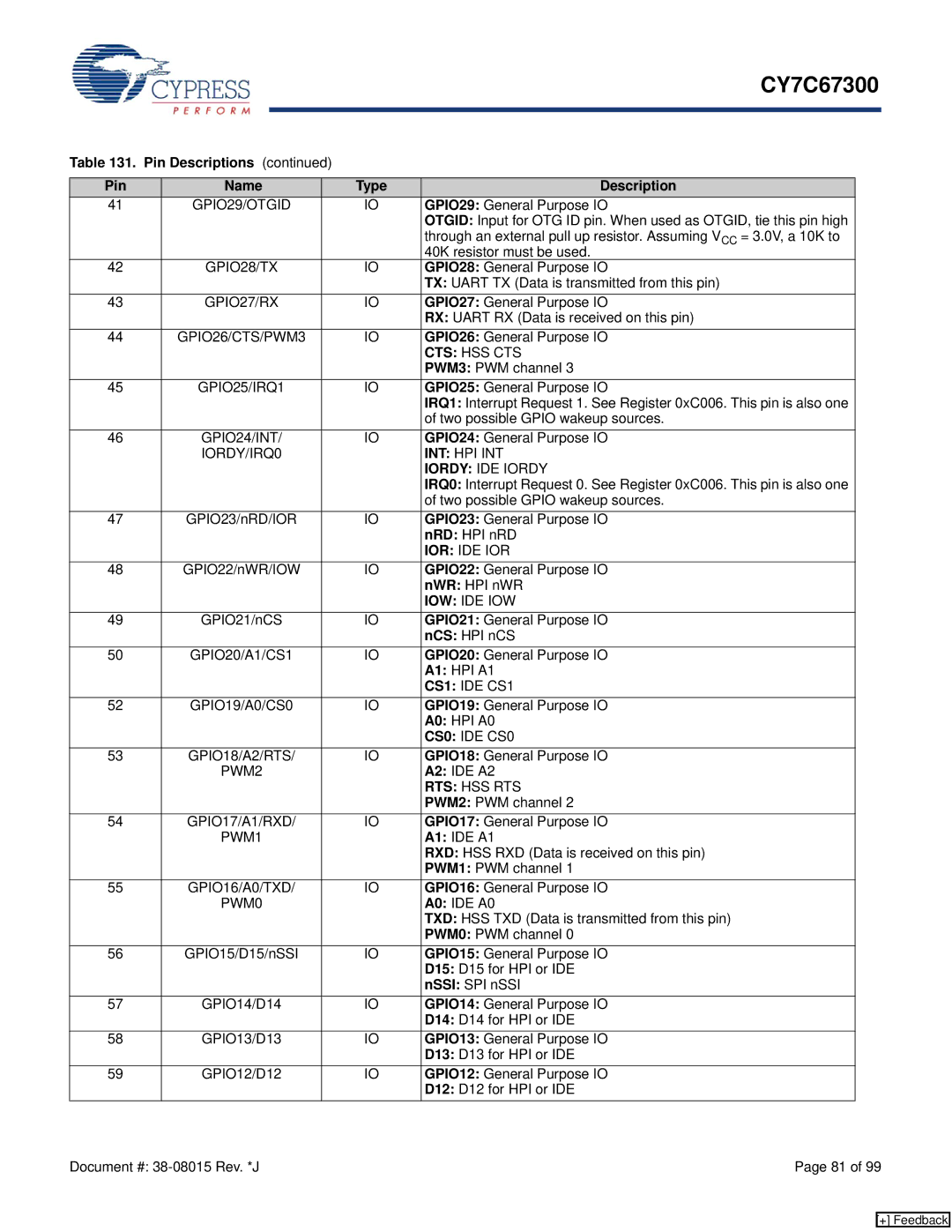
Table 131. Pin Descriptions (continued) |
|
|
| ||
|
|
|
|
|
|
Pin | Name |
| Type | Description |
|
41 | GPIO29/OTGID |
| IO | GPIO29: General Purpose IO |
|
|
|
|
| OTGID: Input for OTG ID pin. When used as OTGID, tie this pin high |
|
|
|
|
| through an external pull up resistor. Assuming VCC = 3.0V, a 10K to |
|
|
|
|
| 40K resistor must be used. |
|
42 | GPIO28/TX |
| IO | GPIO28: General Purpose IO |
|
|
|
|
| TX: UART TX (Data is transmitted from this pin) |
|
43 | GPIO27/RX |
| IO | GPIO27: General Purpose IO |
|
|
|
|
| RX: UART RX (Data is received on this pin) |
|
44 | GPIO26/CTS/PWM3 |
| IO | GPIO26: General Purpose IO |
|
|
|
|
| CTS: HSS CTS |
|
|
|
|
| PWM3: PWM channel 3 |
|
45 | GPIO25/IRQ1 |
| IO | GPIO25: General Purpose IO |
|
|
|
|
| IRQ1: Interrupt Request 1. See Register 0xC006. This pin is also one |
|
|
|
|
| of two possible GPIO wakeup sources. |
|
46 | GPIO24/INT/ |
| IO | GPIO24: General Purpose IO |
|
| IORDY/IRQ0 |
|
| INT: HPI INT |
|
|
|
|
| IORDY: IDE IORDY |
|
|
|
|
| IRQ0: Interrupt Request 0. See Register 0xC006. This pin is also one |
|
|
|
|
| of two possible GPIO wakeup sources. |
|
47 | GPIO23/nRD/IOR |
| IO | GPIO23: General Purpose IO |
|
|
|
|
| nRD: HPI nRD |
|
|
|
|
| IOR: IDE IOR |
|
48 | GPIO22/nWR/IOW |
| IO | GPIO22: General Purpose IO |
|
|
|
|
| nWR: HPI nWR |
|
|
|
|
| IOW: IDE IOW |
|
49 | GPIO21/nCS |
| IO | GPIO21: General Purpose IO |
|
|
|
|
| nCS: HPI nCS |
|
50 | GPIO20/A1/CS1 |
| IO | GPIO20: General Purpose IO |
|
|
|
|
| A1: HPI A1 |
|
|
|
|
| CS1: IDE CS1 |
|
52 | GPIO19/A0/CS0 |
| IO | GPIO19: General Purpose IO |
|
|
|
|
| A0: HPI A0 |
|
|
|
|
| CS0: IDE CS0 |
|
53 | GPIO18/A2/RTS/ |
| IO | GPIO18: General Purpose IO |
|
| PWM2 |
|
| A2: IDE A2 |
|
|
|
|
| RTS: HSS RTS |
|
|
|
|
| PWM2: PWM channel 2 |
|
54 | GPIO17/A1/RXD/ |
| IO | GPIO17: General Purpose IO |
|
| PWM1 |
|
| A1: IDE A1 |
|
|
|
|
| RXD: HSS RXD (Data is received on this pin) |
|
|
|
|
| PWM1: PWM channel 1 |
|
55 | GPIO16/A0/TXD/ |
| IO | GPIO16: General Purpose IO |
|
| PWM0 |
|
| A0: IDE A0 |
|
|
|
|
| TXD: HSS TXD (Data is transmitted from this pin) |
|
|
|
|
| PWM0: PWM channel 0 |
|
56 | GPIO15/D15/nSSI |
| IO | GPIO15: General Purpose IO |
|
|
|
|
| D15: D15 for HPI or IDE |
|
|
|
|
| nSSI: SPI nSSI |
|
57 | GPIO14/D14 |
| IO | GPIO14: General Purpose IO |
|
|
|
|
| D14: D14 for HPI or IDE |
|
58 | GPIO13/D13 |
| IO | GPIO13: General Purpose IO |
|
|
|
|
| D13: D13 for HPI or IDE |
|
59 | GPIO12/D12 |
| IO | GPIO12: General Purpose IO |
|
|
|
|
| D12: D12 for HPI or IDE |
|
Document #: |
| Page 81 of 99 | |||
[+] Feedback