CY7C67300
tAR |
|
tCR |
|
| t RPW |
| tCDH |
tAC | t RDH |
Data Valid
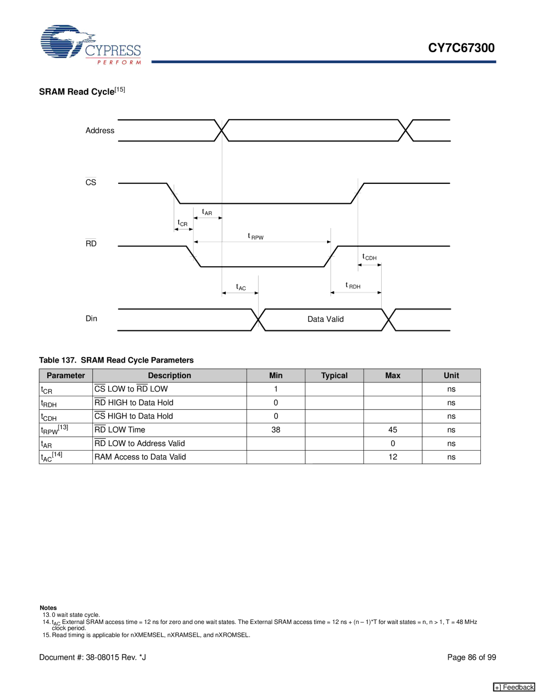
Table 137. SRAM Read Cycle Parameters
Parameter |
|
|
|
|
|
|
| Description | Min | Typical | Max | Unit |
tCR |
|
|
|
|
| LOW to |
| LOW | 1 |
|
| ns |
CS | RD |
|
| |||||||||
tRDH |
|
|
|
|
| HIGH to Data Hold | 0 |
|
| ns | ||
RD |
|
| ||||||||||
tCDH |
|
|
|
| HIGH to Data Hold | 0 |
|
| ns | |||
CS |
|
| ||||||||||
tRPW[13] |
|
|
|
|
| LOW Time | 38 |
| 45 | ns | ||
RD |
| |||||||||||
tAR |
|
|
|
|
| LOW to Address Valid |
|
| 0 | ns | ||
RD |
|
| ||||||||||
tAC[14] |
| RAM Access to Data Valid |
|
| 12 | ns | ||||||
Notes
13.0 wait state cycle.
14.tAC External SRAM access time = 12 ns for zero and one wait states. The External SRAM access time = 12 ns + (n – 1)*T for wait states = n, n > 1, T = 48 MHz clock period.
15.Read timing is applicable for nXMEMSEL, nXRAMSEL, and nXROMSEL.
Document #: | Page 86 of 99 |
[+] Feedback