CY7C67300
Table 14. IDE Throughput
Mode | Actual |
| Actual | ||
Min Cycle Time | Min Cycle Time | Max Transfer Rate | Max Transfer Rate | ||
| |||||
PIO Mode 0 | 600 ns | 30T = 625 ns | 3.33 MB/s | 3.2 MB/s | |
PIO Mode 1 | 383 ns | 20T = 416.7 ns | 5.22 MB/s | 4.8 MB/s | |
PIO Mode 2 | 240 | 13T = 270.8 ns | 8.33 MB/s | 7.38 MB/s | |
PIO Mode 3 | 180 ns | 10T = 208.3 ns | 11.11 MB/s | 9.6 MB/s | |
PIO Mode 4 | 120 ns | 8T = 166.7 ns | 16.67 MB/s | 12.0 MB/s |
T = System clock period = 1/48 MHz.
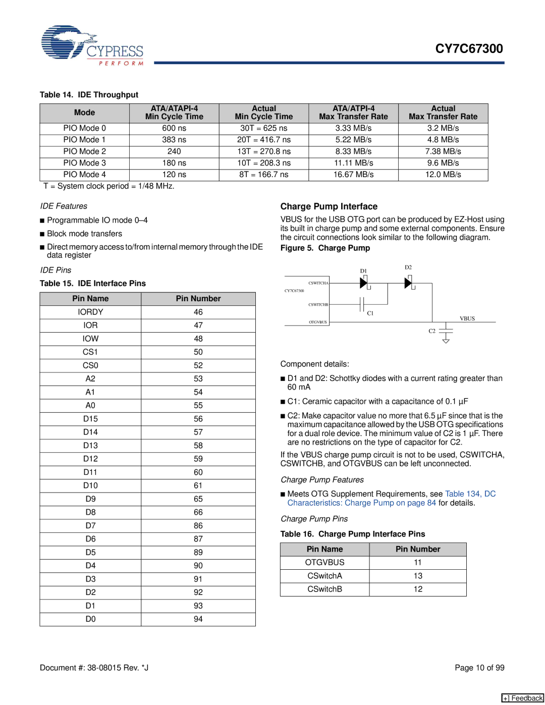
IDE Features | Charge Pump Interface | |
■ Programmable IO mode | VBUS for the USB OTG port can be produced by | |
■ Block mode transfers | its built in charge pump and some external components. Ensure | |
the circuit connections look similar to the following diagram. | ||
■ Direct memory access to/from internal memory through the IDE | ||
Figure 5. Charge Pump | ||
data register |
|
IDE Pins
Table 15. IDE Interface Pins
Pin Name | Pin Number |
IORDY | 46 |
D1D2
CSWITCHA
CY7C67300
CSWITCHB
C1
IOR | 47 |
OTGVBUS
VBUS
IOW | 48 |
CS1 | 50 |
|
|
CS0 | 52 |
|
|
A2 | 53 |
|
|
A1 | 54 |
|
|
A0 | 55 |
|
|
D15 | 56 |
|
|
D14 | 57 |
|
|
D13 | 58 |
|
|
D12 | 59 |
|
|
D11 | 60 |
|
|
D10 | 61 |
|
|
D9 | 65 |
|
|
D8 | 66 |
|
|
D7 | 86 |
|
|
D6 | 87 |
|
|
D5 | 89 |
|
|
D4 | 90 |
|
|
D3 | 91 |
|
|
D2 | 92 |
|
|
D1 | 93 |
|
|
D0 | 94 |
C2
Component details:
■D1 and D2: Schottky diodes with a current rating greater than 60 mA
■C1: Ceramic capacitor with a capacitance of 0.1 µF
■C2: Make capacitor value no more that 6.5 µF since that is the maximum capacitance allowed by the USB OTG specifications for a dual role device. The minimum value of C2 is 1 µF. There are no restrictions on the type of capacitor for C2.
If the VBUS charge pump circuit is not to be used, CSWITCHA, CSWITCHB, and OTGVBUS can be left unconnected.
Charge Pump Features
■Meets OTG Supplement Requirements, see Table 134, DC Characteristics: Charge Pump on page 84 for details.
Charge Pump Pins
Table 16. Charge Pump Interface Pins
Pin Name | Pin Number |
OTGVBUS | 11 |
|
|
CSwitchA | 13 |
|
|
CSwitchB | 12 |
|
|
Document #: | Page 10 of 99 |
[+] Feedback