CY7C67300
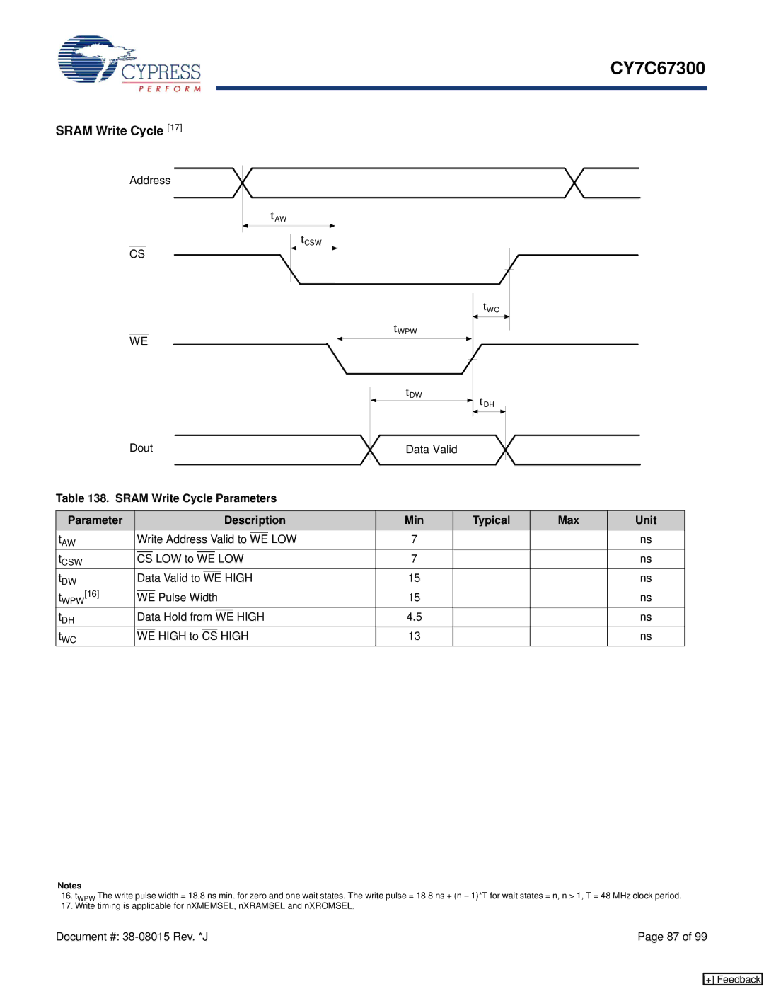
SRAM Write Cycle [17]
Address
tAW
tCSW
CS
WE
Dout
Table 138. SRAM Write Cycle Parameters
tWC
tWPW
tDW | tDH |
|
Data Valid
Parameter |
|
|
|
|
|
|
|
|
|
| Description | Min | Typical | Max | Unit | |||
tAW |
| Write Address Valid to |
| LOW | 7 |
|
| ns | ||||||||||
WE |
|
| ||||||||||||||||
tCSW |
|
|
| LOW to |
|
|
|
|
| LOW | 7 |
|
| ns | ||||
CS | WE |
|
| |||||||||||||||
tDW |
| Data Valid to |
|
|
|
| HIGH | 15 |
|
| ns | |||||||
WE |
|
| ||||||||||||||||
tWPW[16] |
|
|
| Pulse Width | 15 |
|
| ns | ||||||||||
WE |
|
| ||||||||||||||||
tDH |
| Data Hold from |
|
|
| HIGH | 4.5 |
|
| ns | ||||||||
WE |
|
| ||||||||||||||||
tWC |
|
|
| HIGH to |
|
|
|
| HIGH | 13 |
|
| ns | |||||
WE | CS |
|
| |||||||||||||||
Notes
16.tWPW The write pulse width = 18.8 ns min. for zero and one wait states. The write pulse = 18.8 ns + (n – 1)*T for wait states = n, n > 1, T = 48 MHz clock period.
17.Write timing is applicable for nXMEMSEL, nXRAMSEL and nXROMSEL.
Document #: | Page 87 of 99 |
[+] Feedback