CHAPTER 2
B.Laser Control Circuit
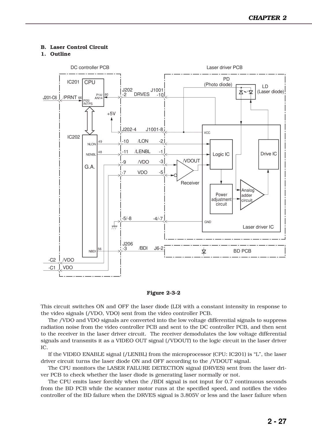
1. Outline
DC controller PCB | Laser driver PCB |
IC201
/PRNT 66
IC202
CPU
P14/ 80
AN14 ![]()
P05/
INTPS
+5V
49
NLON
48
NENBL
G.A.
J202 | J1001 |
DRVES |
PD |
|
(Photo diode) | LD |
| |
| (Laser diode) |
VCC |
|
Logic IC | Drive IC |
/VDOUT |
|
Receiver |
|
Power | Analog |
adder | |
adjustment | circuit |
circuit |
|
GND |
|
| Laser driver IC |
56 |
NBDI |
/VDO |
VDO |
J206 | /BDI |
|
| ||
| BD PCB | ||||
| |||||
|
|
|
|
| |
|
|
|
|
|
|
Figure
This circuit switches ON and OFF the laser diode (LD) with a constant intensity in response to the video signals (/VDO, VDO) sent from the video controller PCB.
The /VDO and VDO signals are converted into the low voltage differential signals to suppress radiation noise from the video controller PCB and sent to the DC controller PCB, and then sent to the receiver in the laser driver circuit. The receiver demodulates the low voltage differential signals and transmits it as a VIDEO OUT signal (/VDOUT) to the logic circuit in the laser driver IC.
If the VIDEO ENABLE signal (/LENBL) from the microprocessor (CPU: IC201) is “L”, the laser driver circuit turns the laser diode ON and OFF according to the /VDOUT signal.
The CPU monitors the LASER FAILURE DETECTION signal (DRVES) sent from the laser dri- ver PCB to check whether the laser diode is generating laser normally or not.
The CPU emits laser forcibly when the /BDI signal is not input for 0.7 continuous seconds from the BD PCB while the scanner motor runs at the specified speed, and notifies the video controller of the BD failure when the DRVES signal is 3.805V or less and the laser failure when
2 - 27