CHAPTER 2
Laser/scanner unit |
|
|
|
|
|
|
|
|
|
|
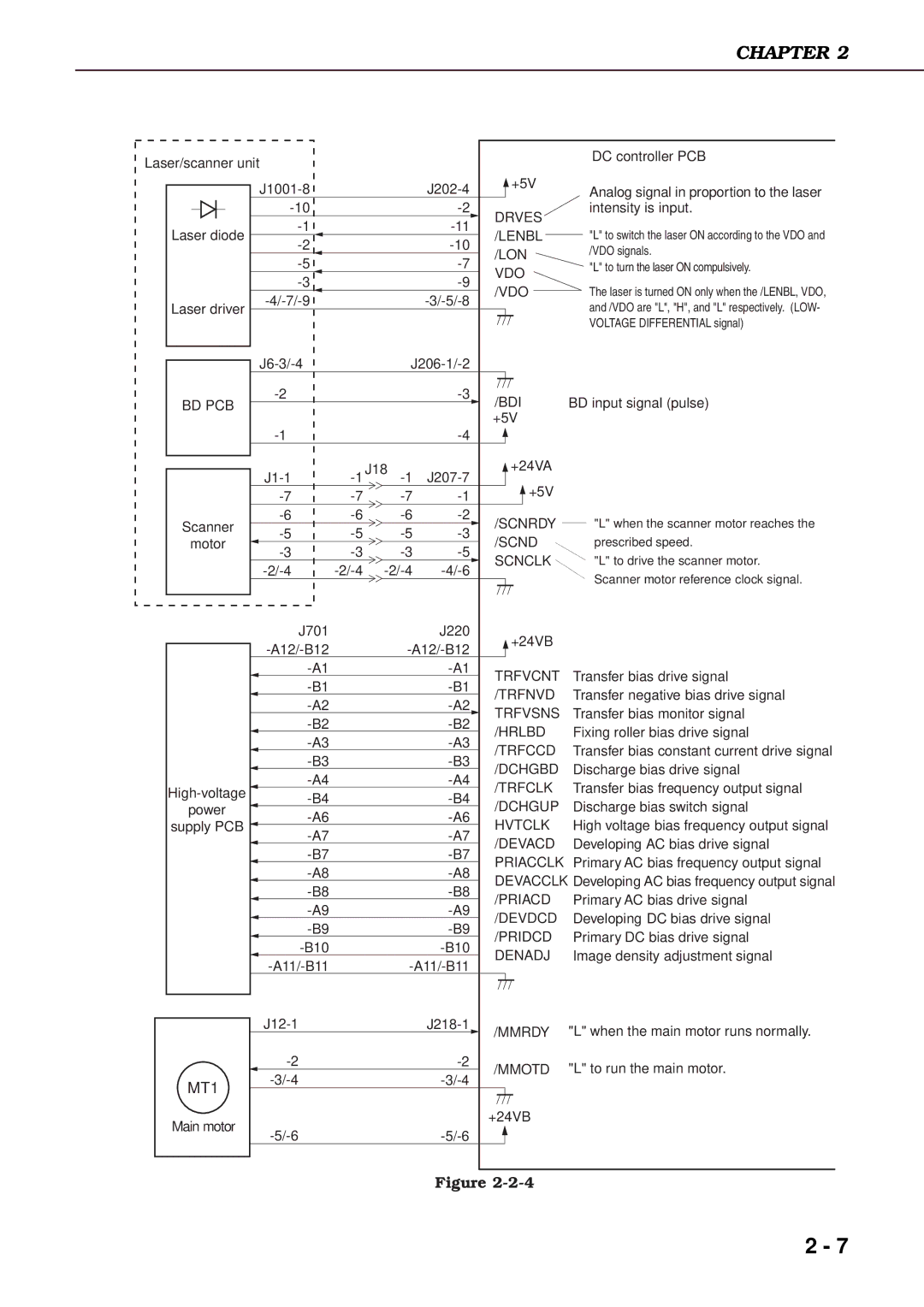
| DC controller PCB | |||||
|
|
|
|
|
|
|
|
|
|
|
| ||||||
|
|
|
|
|
|
|
|
|
|
| +5V | Analog signal in proportion to the laser | |||||
|
|
|
|
|
|
|
|
|
|
|
|
|
| ||||
|
|
|
|
|
|
|
|
|
| DRVES | intensity is input. | ||||||
|
|
|
|
|
|
|
|
| |||||||||
|
| Laser diode |
|
|
|
|
|
|
| ||||||||
|
|
|
|
|
|
|
| /LENBL | "L" to switch the laser ON according to the VDO and | ||||||||
|
|
|
|
|
|
|
| ||||||||||
|
|
|
|
|
|
|
|
|
| /LON | /VDO signals. | ||||||
|
|
|
|
|
|
|
|
|
| ||||||||
|
|
|
|
|
|
|
|
|
| VDO | "L" to turn the laser ON compulsively. | ||||||
|
|
|
|
|
|
|
|
|
|
| |||||||
|
|
|
|
|
|
|
|
|
| /VDO | The laser is turned ON only when the /LENBL, VDO, | ||||||
|
|
|
|
|
|
|
|
|
| ||||||||
|
| Laser driver |
|
|
|
|
|
|
|
|
|
|
| and /VDO are "L", "H", and "L" respectively. (LOW- | |||
|
|
|
|
|
|
|
|
|
|
|
|
|
|
| |||
|
|
|
|
|
|
|
|
|
|
|
|
| VOLTAGE DIFFERENTIAL signal) | ||||
|
|
|
|
|
|
|
|
|
|
|
|
|
| ||||
|
|
|
|
|
|
|
|
|
|
|
|
|
| ||||
|
|
|
|
|
|
|
|
|
|
|
|
|
| ||||
|
|
|
|
|
|
|
|
|
|
|
|
|
|
|
| ||
|
| BD PCB |
|
|
|
|
|
| /BDI | BD input signal (pulse) | |||||||
|
|
|
|
|
|
|
|
|
| ||||||||
|
|
|
|
|
|
|
|
|
|
|
| +5V |
| ||||
|
|
|
|
|
|
|
|
|
|
|
| +24VA |
| ||||
|
|
|
|
|
|
|
|
|
|
|
| ||||||
|
|
|
|
|
|
|
|
| |||||||||
|
|
|
|
|
|
|
|
| |||||||||
|
|
|
|
|
|
|
|
|
| +5V |
| ||||||
|
|
|
|
|
|
|
|
|
|
|
|
| |||||
|
|
|
|
|
|
|
|
|
|
|
|
| |||||
|
|
|
|
|
|
|
|
|
|
|
|
|
| ||||
|
| Scanner |
|
|
|
| /SCNRDY | "L" when the scanner motor reaches the | |||||||||
|
|
|
|
|
| ||||||||||||
|
|
|
|
|
| ||||||||||||
|
|
|
|
|
| ||||||||||||
|
|
|
|
|
| ||||||||||||
|
| motor |
|
|
|
| /SCND | prescribed speed. | |||||||||
|
|
|
|
|
| ||||||||||||
|
|
|
|
|
| ||||||||||||
|
|
|
|
|
| ||||||||||||
|
|
|
|
|
|
|
| SCNCLK | "L" to drive the scanner motor. | ||||||||
|
|
|
|
|
|
|
| ||||||||||
|
|
|
|
|
|
|
| ||||||||||
|
|
|
|
|
|
|
| ||||||||||
|
|
|
|
|
|
|
|
|
|
|
|
| Scanner motor reference clock signal. | ||||
|
|
|
|
|
|
|
|
|
|
|
|
| |||||
|
|
|
|
|
| J701 |
|
|
| J220 |
|
| +24VB |
| |||
|
|
|
|
|
|
|
|
|
|
|
| ||||||
|
|
|
|
|
|
|
|
|
|
| |||||||
|
|
|
|
|
|
|
|
|
|
| |||||||
|
|
|
|
|
|
|
|
|
|
|
|
|
| ||||
|
|
|
|
|
|
|
|
| TRFVCNT | Transfer bias drive signal | |||||||
|
|
|
|
|
|
|
|
| |||||||||
|
|
|
|
|
|
|
|
| /TRFNVD | Transfer negative bias drive signal | |||||||
|
|
|
|
|
|
|
|
| |||||||||
|
|
|
|
|
|
|
|
| TRFVSNS | Transfer bias monitor signal | |||||||
|
|
|
|
|
|
|
|
| |||||||||
|
|
|
|
|
|
|
|
| /HRLBD | Fixing roller bias drive signal | |||||||
|
|
|
|
|
|
|
|
| |||||||||
|
|
|
|
|
|
|
|
| /TRFCCD | Transfer bias constant current drive signal | |||||||
|
|
|
|
|
|
|
|
| |||||||||
|
|
|
|
|
|
|
|
| /DCHGBD | Discharge bias drive signal | |||||||
|
|
|
|
|
|
|
|
| |||||||||
|
|
|
|
|
|
| /TRFCLK | Transfer bias frequency output signal | |||||||||
|
|
|
|
|
|
| |||||||||||
|
|
|
|
|
|
| /DCHGUP | Discharge bias switch signal | |||||||||
|
| power |
|
|
|
|
| ||||||||||
|
|
|
|
|
|
| |||||||||||
|
| supply PCB |
|
|
|
|
| HVTCLK | High voltage bias frequency output signal | ||||||||
|
|
|
|
|
|
| |||||||||||
|
|
|
|
|
|
|
|
| /DEVACD | Developing AC bias drive signal | |||||||
|
|
|
|
|
|
|
|
| |||||||||
|
|
|
|
|
|
|
|
| PRIACCLK | Primary AC bias frequency output signal | |||||||
|
|
|
|
|
|
|
|
| |||||||||
|
|
|
|
|
|
|
|
| DEVACCLK Developing AC bias frequency output signal | ||||||||
|
|
|
|
|
|
|
|
| |||||||||
|
|
|
|
|
|
|
|
| /PRIACD | Primary AC bias drive signal | |||||||
|
|
|
|
|
|
|
|
| |||||||||
|
|
|
|
|
|
|
|
| /DEVDCD | Developing DC bias drive signal | |||||||
|
|
|
|
|
|
|
|
| |||||||||
|
|
|
|
|
|
|
|
| /PRIDCD | Primary DC bias drive signal | |||||||
|
|
|
|
|
|
|
|
| |||||||||
|
|
|
|
|
|
|
|
| DENADJ | Image density adjustment signal | |||||||
|
|
|
|
|
|
|
| ||||||||||
|
|
|
|
|
|
|
|
|
|
|
|
|
| ||||
|
|
|
|
|
|
|
|
|
|
|
|
|
| "L" when the main motor runs normally. | |||
|
|
|
|
|
|
|
|
| /MMRDY | ||||||||
|
|
|
|
|
|
|
|
| |||||||||
|
|
|
|
|
|
|
|
| |||||||||
|
|
|
|
|
|
|
|
|
| ||||||||
|
|
|
|
|
|
|
|
|
| /MMOTD | "L" to run the main motor. | ||||||
|
| MT1 |
|
|
|
|
|
| |||||||||
|
|
|
|
|
|
|
|
|
|
|
|
|
| ||||
|
|
|
|
|
|
|
|
|
|
|
|
|
|
|
| ||
|
| Main motor |
|
|
|
|
|
|
|
| +24VB |
| |||||
|
|
|
|
|
|
|
|
|
|
|
|
|
| ||||
|
|
|
|
|
|
|
|
|
|
|
|
|
|
|
| ||
|
|
|
|
|
|
|
|
|
|
|
|
|
|
|
|
|
|
|
|
|
|
|
|
|
|
|
|
|
|
|
|
|
|
|
|
Figure
2 - 7