P R E L I M I N A R Y
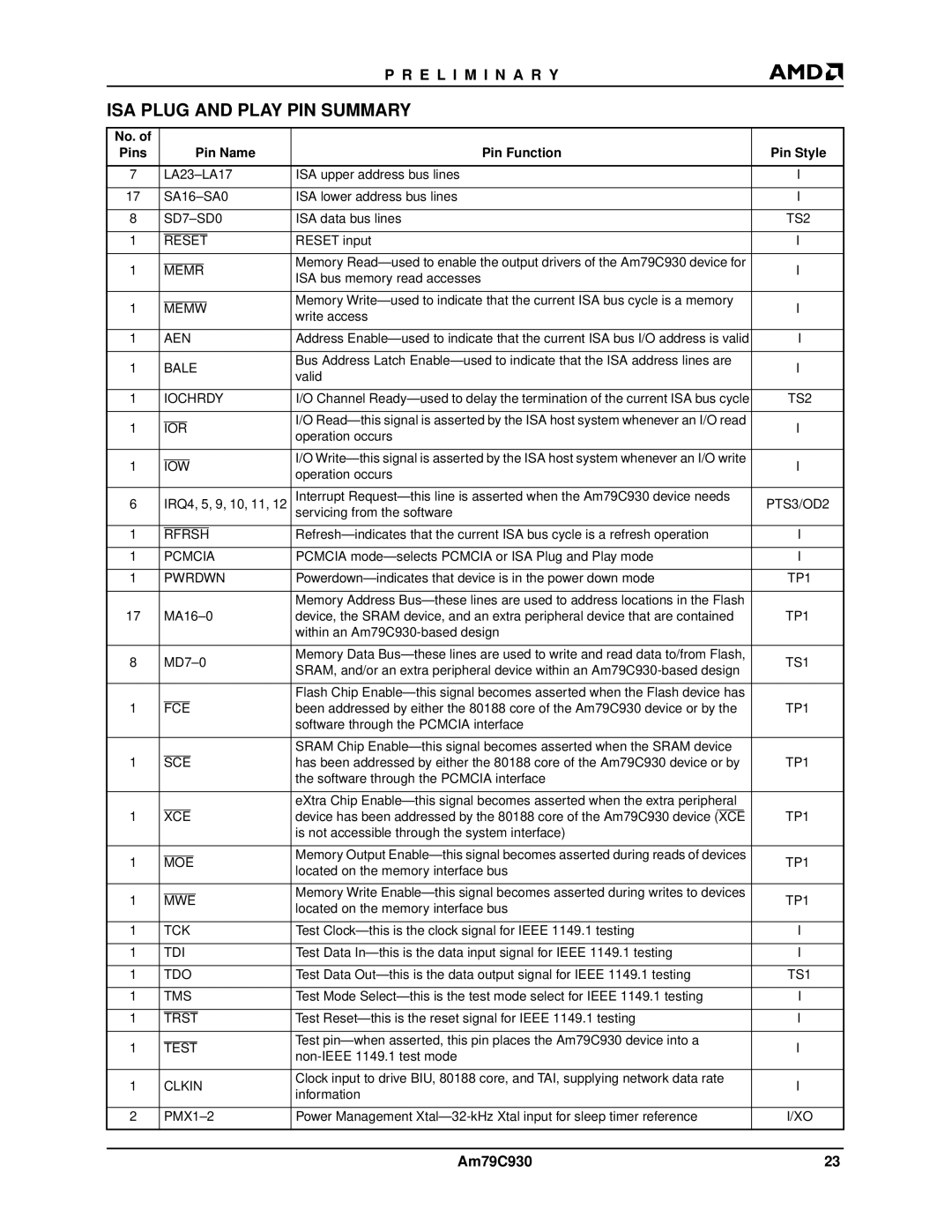
ISA PLUG AND PLAY PIN SUMMARY
No. of |
|
|
|
|
|
|
|
|
|
|
|
|
|
|
|
Pins |
|
|
|
|
| Pin Name | Pin Function | Pin Style | |||||||
|
|
|
|
| |||||||||||
7 |
| ISA upper address bus lines | I | ||||||||||||
|
|
|
|
| |||||||||||
17 |
| ISA lower address bus lines | I | ||||||||||||
|
|
|
|
| |||||||||||
8 |
|
| ISA data bus lines | TS2 | |||||||||||
|
|
|
|
|
|
|
|
|
|
|
|
|
| ||
1 |
|
|
|
|
|
|
|
|
|
|
| RESET input | I | ||
RESET | |||||||||||||||
|
|
|
|
|
|
|
|
|
|
|
|
|
| ||
|
|
|
|
|
|
|
|
|
|
|
| Memory | I | ||
1 |
| MEMR | |||||||||||||
| ISA bus memory read accesses | ||||||||||||||
|
|
|
|
|
|
|
|
|
|
|
|
| |||
|
|
|
|
|
|
|
|
|
|
|
|
|
| ||
|
|
|
|
|
|
|
|
|
|
|
| Memory | I | ||
1 |
| MEMW | |||||||||||||
| write access | ||||||||||||||
|
|
|
|
|
|
|
|
|
|
|
|
| |||
|
|
|
|
| |||||||||||
1 |
| AEN | Address | I | |||||||||||
|
|
|
|
|
|
|
|
|
|
|
|
|
| ||
1 |
| BALE | Bus Address Latch | I | |||||||||||
| valid | ||||||||||||||
|
|
|
|
|
|
|
|
|
|
|
|
| |||
|
|
|
|
| |||||||||||
1 |
| IOCHRDY | I/O Channel | TS2 | |||||||||||
|
|
|
|
|
|
|
|
|
|
|
|
|
| ||
|
|
|
|
|
|
|
|
|
|
|
| I/O | I | ||
1 |
| IOR | |||||||||||||
| operation occurs | ||||||||||||||
|
|
|
|
|
|
|
|
|
|
|
|
| |||
|
|
|
|
|
|
|
|
|
|
|
|
|
| ||
|
|
|
|
|
|
|
|
|
|
|
| I/O | I | ||
1 |
| IOW | |||||||||||||
| operation occurs | ||||||||||||||
|
|
|
|
|
|
|
|
|
|
|
|
| |||
|
|
|
|
|
|
|
|
|
|
|
|
|
| ||
6 |
| IRQ4, 5, 9, 10, 11, 12 | Interrupt | PTS3/OD2 | |||||||||||
| servicing from the software | ||||||||||||||
|
|
|
|
|
|
|
|
|
|
| |||||
1 |
|
|
|
|
|
|
|
|
|
|
| I | |||
RFRSH | |||||||||||||||
|
|
|
|
| |||||||||||
1 |
| PCMCIA | PCMCIA | I | |||||||||||
|
|
|
|
| |||||||||||
1 |
| PWRDWN | TP1 | ||||||||||||
|
|
|
|
|
|
|
|
|
|
|
|
|
| ||
|
|
|
|
|
|
|
|
|
|
|
| Memory Address |
| ||
17 |
| device, the SRAM device, and an extra peripheral device that are contained | TP1 | ||||||||||||
|
|
|
|
|
|
|
|
|
|
|
| within an |
| ||
|
|
|
|
|
|
|
|
|
|
|
|
|
| ||
8 |
| Memory Data | TS1 | ||||||||||||
| SRAM, and/or an extra peripheral device within an | ||||||||||||||
|
|
|
|
|
|
|
|
|
|
|
|
| |||
|
|
|
|
|
|
|
|
|
|
|
|
|
| ||
|
|
|
|
|
|
|
|
|
|
|
| Flash Chip |
| ||
1 |
| FCE |
|
|
|
|
| been addressed by either the 80188 core of the Am79C930 device or by the | TP1 | ||||||
|
|
|
|
|
|
|
|
|
|
|
| software through the PCMCIA interface |
| ||
|
|
|
|
|
|
|
|
|
|
|
|
|
| ||
|
|
|
|
|
|
|
|
|
|
|
| SRAM Chip |
| ||
1 |
|
|
|
|
|
| has been addressed by either the 80188 core of the Am79C930 device or by | TP1 | |||||||
SCE | |||||||||||||||
|
|
|
|
|
|
|
|
|
|
|
| the software through the PCMCIA interface |
| ||
|
|
|
|
|
|
|
|
|
|
|
|
|
| ||
|
|
|
|
|
|
|
|
|
|
|
| eXtra Chip |
| ||
1 |
|
|
|
|
|
| device has been addressed by the 80188 core of the Am79C930 device |
|
| TP1 | |||||
XCE | (XCE | ||||||||||||||
|
|
|
|
|
|
|
|
|
|
|
| is not accessible through the system interface) |
| ||
|
|
|
|
|
|
|
|
|
|
|
|
|
| ||
|
|
|
|
|
|
|
|
|
|
|
| Memory Output | TP1 | ||
1 |
| MOE | |||||||||||||
| located on the memory interface bus | ||||||||||||||
|
|
|
|
|
|
|
|
|
|
|
|
| |||
|
|
|
|
|
|
|
|
|
|
|
|
|
| ||
|
|
|
|
|
|
|
|
|
|
|
| Memory Write | TP1 | ||
1 |
| MWE | |||||||||||||
| located on the memory interface bus | ||||||||||||||
|
|
|
|
|
|
|
|
|
|
|
|
| |||
|
|
|
|
| |||||||||||
1 |
| TCK | Test | I | |||||||||||
|
|
|
|
| |||||||||||
1 |
| TDI | Test Data | I | |||||||||||
|
|
|
|
| |||||||||||
1 |
| TDO | Test Data | TS1 | |||||||||||
|
|
|
|
| |||||||||||
1 |
| TMS | Test Mode | I | |||||||||||
|
|
|
|
|
|
| |||||||||
1 |
|
|
|
|
|
|
|
| Test | I | |||||
TRST | |||||||||||||||
|
|
|
|
|
|
|
|
|
|
|
|
|
| ||
|
|
|
|
|
|
|
|
|
|
|
| Test | I | ||
1 |
| TEST | |||||||||||||
| |||||||||||||||
|
|
|
|
|
|
|
|
|
|
|
|
| |||
|
|
|
|
|
|
|
|
|
|
|
|
|
| ||
1 |
| CLKIN | Clock input to drive BIU, 80188 core, and TAI, supplying network data rate | I | |||||||||||
| information | ||||||||||||||
|
|
|
|
|
|
|
|
|
|
|
|
| |||
|
|
|
|
| |||||||||||
2 |
| Power Management | I/XO | ||||||||||||
|
|
|
|
|
|
|
|
|
|
|
|
|
|
|
|
|
|
|
|
|
|
|
|
|
|
|
|
|
|
|
|
|
|
|
|
|
|
|
|
|
|
|
| Am79C930 | 23 | ||