| AMD |
| P R E L I M I N A R Y | |
|
|
|
|
|
2 | INT2EC | 0 | Interrupt to Embedded Controller. When INT2EC is set to a 1, an | |
|
|
| interrupt is sent to the 80188 core. INT2EC will stay set at 1 until the | |
|
|
| 80188 core clears this bit by writing a 1 to bit 3 of the MIR0 register. | |
|
|
| Writing a 0 to INT2EC will have no effect on the value of INT2EC. | |
1 | ENECINT | 0 | Enable Embedded Controller Interrupts. When set to 1, enables | |
|
|
| 80188 | |
|
|
| they will appear as interrupts on the ECINT bit of SIR0 and also on | |
|
|
| the system interface interrupt pin. When set to 0, no 80188 core- | |
|
|
| generated interrupts will be passed to the BIU. | |
0 | DAM | 0 | Direct Access Mode. DAM is a | |
|
|
| 80188 embedded controller has set the SIDA bit of MIR0 (bit 7), | |
|
|
| thereby giving the system interface direct accessibility to the mem- | |
|
|
| ory interface of the Am79C930 device. The 80188 embedded con- | |
|
|
| troller should only give such access to the system interface when | |
|
|
| the 80188 follows such action with a HALT instruction, otherwise | |
80188 accesses to the memory interface may interfere with the di- rect access given to the system interface. This mode can be re- leased if the system interface interrupts the 80188. An 80188 interrupt will cause the 80188 to exit the HALT state and will allow the 80188 to reset the SIDA bit to 0. The value of the DAM bit is the same as the value of the SIDA bit of MIR0 (bit 7).
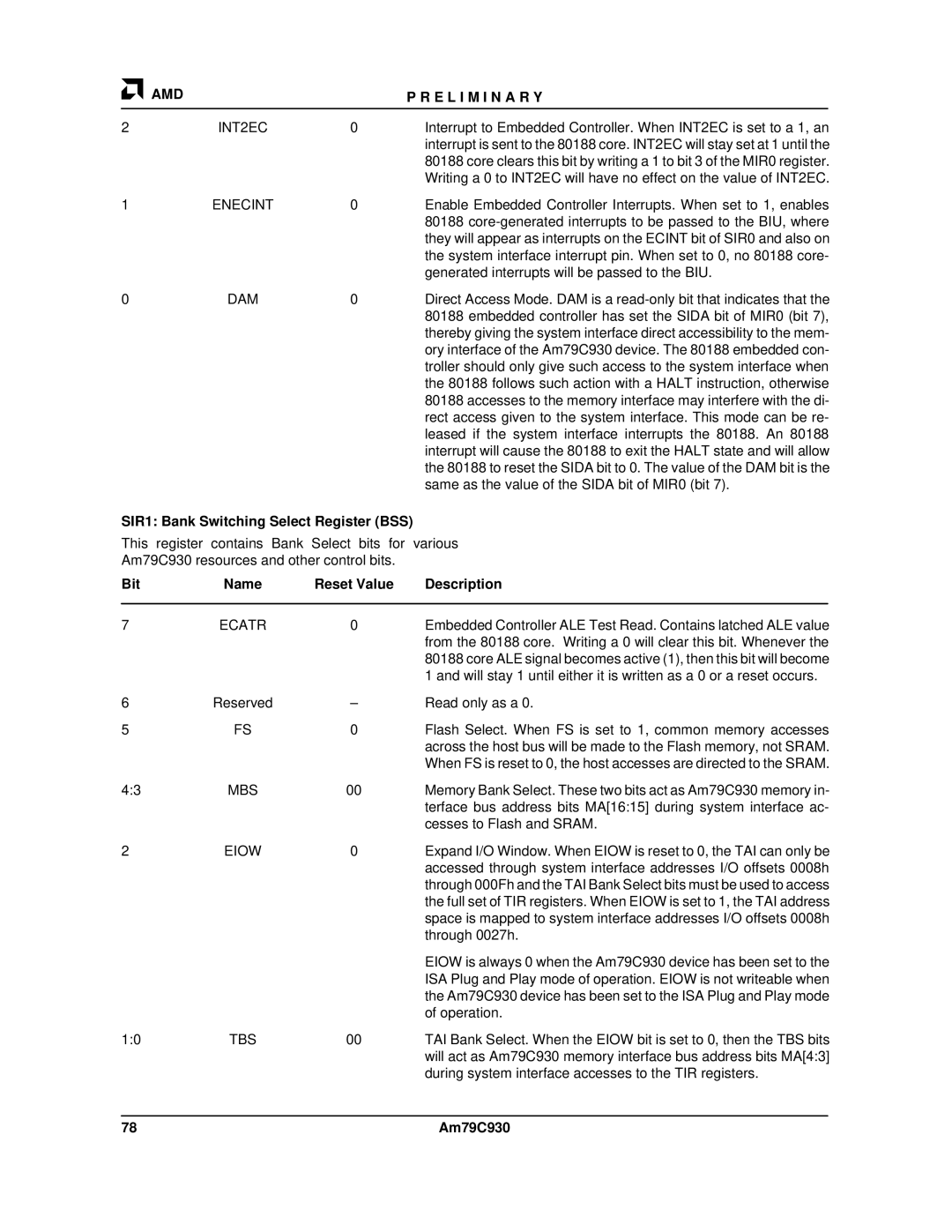
SIR1: Bank Switching Select Register (BSS)
This register contains Bank Select bits for various
Am79C930 resources and other control bits.
Bit | Name | Reset Value | Description | |
|
|
|
|
|
7 | ECATR | 0 | Embedded Controller ALE Test Read. Contains latched ALE value | |
|
|
| from the 80188 core. Writing a 0 will clear this bit. Whenever the | |
|
|
| 80188 core ALE signal becomes active (1), then this bit will become | |
|
|
| 1 and will stay 1 until either it is written as a 0 or a reset occurs. | |
6 | Reserved | – | Read only as a 0. | |
5 | FS | 0 | Flash Select. When FS is set to 1, common memory accesses | |
|
|
| across the host bus will be made to the Flash memory, not SRAM. | |
|
|
| When FS is reset to 0, the host accesses are directed to the SRAM. | |
4:3 | MBS | 00 | Memory Bank Select. These two bits act as Am79C930 memory in- | |
|
|
| terface bus address bits MA[16:15] during system interface ac- | |
|
|
| cesses to Flash and SRAM. | |
2 | EIOW | 0 | Expand I/O Window. When EIOW is reset to 0, the TAI can only be | |
|
|
| accessed through system interface addresses I/O offsets 0008h | |
|
|
| through 000Fh and the TAI Bank Select bits must be used to access | |
|
|
| the full set of TIR registers. When EIOW is set to 1, the TAI address | |
|
|
| space is mapped to system interface addresses I/O offsets 0008h | |
|
|
| through 0027h. | |
|
|
| EIOW is always 0 when the Am79C930 device has been set to the | |
|
|
| ISA Plug and Play mode of operation. EIOW is not writeable when | |
|
|
| the Am79C930 device has been set to the ISA Plug and Play mode | |
|
|
| of operation. | |
1:0 | TBS | 00 | TAI Bank Select. When the EIOW bit is set to 0, then the TBS bits | |
|
|
| will act as Am79C930 memory interface bus address bits MA[4:3] | |
|
|
| during system interface accesses to the TIR registers. | |
|
|
|
|
|
78 |
|
| Am79C930 | |
